SLVA275C january 2010 – may 2023 UCD9081
- Abstract
- Trademarks
- 1Introduction
- 2Hardware
- 3Software
-
4User Configuration
- 4.1 Configuration Parameter Memory Map
- 4.2
Configuration Parameter Detail
- 4.2.1 GpDir
- 4.2.2 NegateEnablePolarity
- 4.2.3 SeqEventPending
- 4.2.4 SequenceEventParameters
- 4.2.5 SequenceEventLink
- 4.2.6 SequenceEventData
- 4.2.7 DependencyMasks
- 4.2.8 UnderVoltageThresholds
- 4.2.9 OverVoltageThresholds
- 4.2.10 RampTime
- 4.2.11 OutOfRegulationWidth
- 4.2.12 UnsequenceTime
- 4.2.13 EnablePolarity
- 4.2.14 SaveRailLog
- 4.2.15 ReferenceSelect
- 4.2.16 LastUnusedSeq
- 4.2.17 IgnoreGlitchAlarms
- 4.2.18 IgnoreFlashErrorLog
- 4.2.19 Checksum
- 5Additional Considerations
- 6References
- 7Revision History
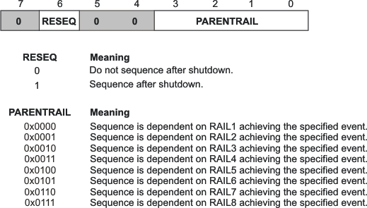
4.2.5 SequenceEventLink
The SequenceEventLink field allows a parent rail (monitored input) to be specified for each ENx and GPOx output. The RESEQ bit (sequence after shutdown) allows an enable or GPO to be marked to sequence the system (as defined by the current sequencer configuration) after it has been shut down. The address map for these registers is as follows:
| Address | Size | Default Value | Description |
|---|---|---|---|
| 0xE08C | 1 | 0x01 | Rail 1 parent rail identifier and resequence indicator |
| 0xE08D | 1 | 0x00 | Rail 2 parent rail identifier and resequence indicator |
| 0xE08E | 1 | 0x01 | Rail 3 parent rail identifier and resequence indicator |
| 0xE08F | 1 | 0x04 | Rail 4 parent rail identifier and resequence indicator |
| 0xE090 | 1 | 0x01 | Rail 5 parent rail identifier and resequence indicator |
| 0xE091 | 1 | 0x04 | Rail 6 parent rail identifier and resequence indicator |
| 0xE092 | 1 | 0x05 | Rail 7 parent rail identifier and resequence indicator |
| 0xE093 | 1 | 0x06 | Rail 8 parent rail identifier and resequence indicator |
| 0xE094 | 1 | 0x00 | GPO1 parent rail identifier and resequence indicator |
| 0xE095 | 1 | 0x00 | GPO2 parent rail identifier and resequence indicator |
| 0xE096 | 1 | 0x00 | GPO3 parent rail identifier and resequence indicator |
| 0xE097 | 1 | 0x00 | GPO4 parent rail identifier and resequence indicator |
The format of each register is as follows: