SNOA961A February 2017 – February 2023 LDC2112 , LDC2114 , LDC3114 , LDC3114-Q1
- Inductive Touch System Design Guide for HMI Button Applications
- 1Mechanical Design
- 2Sensor Design
- 3Summary
- 4Revision History
2.4.6 Multi-Layer Design
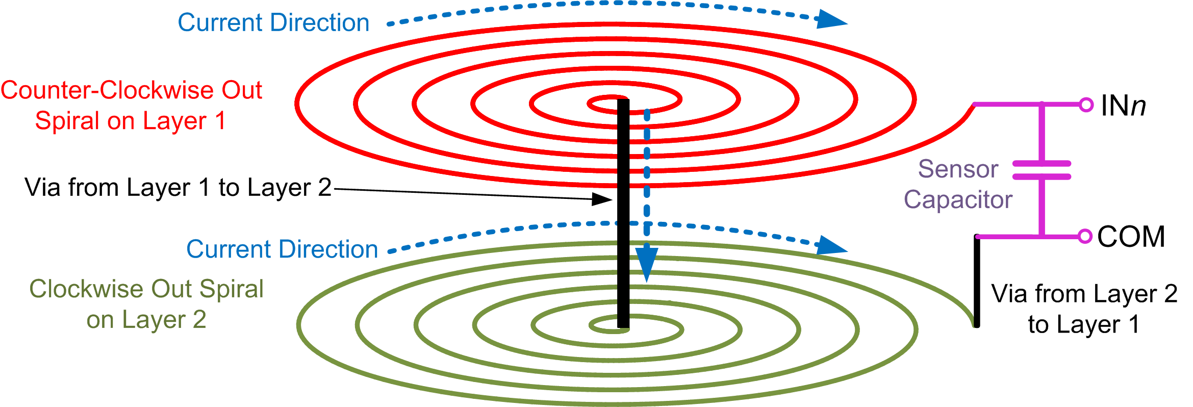
The inductance of a sensor is a function of the area, and the number of windings, and target distance. With many inductive touch applications, the desired physical size of the buttons may be 3-mm in diameter or smaller. The low total inductance of smaller sensors may result in a sensor frequency which is outside the design space of the LDC. By using multiple layers of alternating rotation sensors, the total inductance, due to additional mutual inductance between layers, is significantly higher compared to a single layer design.
 Figure 2-8 2-Layer Sensor Design
For most applications, 2-layer or 4-layer designs are sufficient. While a 4-layer sensor is more complex and expensive compared to a similar geometry 2-layer sensor, the LDC211x and LDC3114 can effectively drive a physically smaller 4-layer sensor, as shown in #GUID-1D47ED31-A7E1-4356-B584-99B68CC4AF6D/T4726003-68.
Use of a single layer sensor is generally not as effective, as the mutual coupling between layers in a multilayer sensor provides a significant increase in the sensor inductance. In addition, there needs to be a second routing to bring the sensor current out from the center of the sensor back to the LDC.
| AVAILABLE SPACING DISTANCE BETWEEN TURNS | NUMBER OF LAYERS | MINIMUM VIA SIZE | MINIMUM SENSOR WIDTH |
|---|---|---|---|
| 4 mil (0.1016 mm) | 2 | 15 mil (0.4 mm) | 2.85 mm |
| 4 mil (0.1016 mm) | 4 | 15 mil (0.4 mm) | 2.30 mm |
| 3 mil (0.076 mm) | 2 | 15 mil (0.4 mm) | 2.05 mm |
| 3 mil (0.076 mm) | 4 | 15 mil (0.4 mm) | 1.91 mm |
| 2 mil (0.051 mm) | 2 | 15 mil (0.4 mm) | 1.65 mm |
| 2 mil (0.051 mm) | 4 | 15 mil (0.4 mm) | 1.53 mm |
| 2 mil (0.051 mm) | 4 | 12 mil (0.305 mm) | 1.38 mm |
Minimum sensor width of a fixed 8-mm sensor length with a target distance of 0.2 mm. These sensors have not been evaluated for performance. These sensors assume a 1-mil (25 µm) dielectric thickness between layers.