SNOA961A February 2017 – February 2023 LDC2112 , LDC2114 , LDC3114 , LDC3114-Q1
- Inductive Touch System Design Guide for HMI Button Applications
- 1Mechanical Design
- 2Sensor Design
- 3Summary
- 4Revision History
2.5 Example Sensor
For this example, a dual sensor design is presented. #T4726003-77 shows the sensors are 2.85 mm × 8 mm in size with eight turns. The traces are 0.25 oz-cu (9 µm) thick, are 75 µm wide and have a spacing of 50 µm. The sensor free-space inductance is approximately 1.3 µH, and has a 47-pF sensor capacitor. When mounted, the sensor inductance decreases due to interaction with the conductive target.
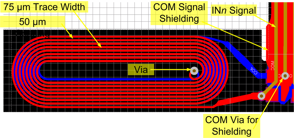 Figure 2-13 Sensor
Racetrack Routing
Figure 2-13 Sensor
Racetrack RoutingThe parameters of this sensor were estimated using the Racetrack Inductor Designer tab on the LDC Calculations Tool. #T4726003-78 is an example of the tool entries used to design the sensor described here. Note that the tool provides estimates of the sensor parameters such as RS, RP, Q, L, and frequency, based on GUID-6AC968E3-0011-4198-B542-46F8F31E3EDE.html#X6785, GUID-9C1D6CFD-667C-4F3D-BDFE-DE70B8873788.html#X1756, and GUID-5C771CC9-1180-4B3C-97F1-5477D165F8C1.html#X3711.
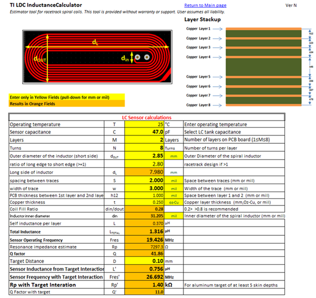 Figure 2-14 Racetrack
Inductor Design Tab of the LDC Calculations Tool
Figure 2-14 Racetrack
Inductor Design Tab of the LDC Calculations ToolThe tool output includes estimates for both free space parameters (no target present) and their values when the sensor is mounted in the system with a target close by. As seen in Table 2-2, the sensor parameters are within the LDC211x/LDC3114 operating space when the sensor is mounted.
| SENSOR PARAMETERS | SENSOR IN FREE SPACE | SENSOR MOUNTED | LDC211x/LDC3114 OPERATING SPACE |
|---|---|---|---|
| Sensor Inductance | 1.3 µH | 0.76 µH | |
| Sensor Capacitance | 47 pF | 47 pF | |
| Sensor Frequency | 19.4 MHz | 26.7 MHz | 1 MHz – 30
MHz (LDC211x) 5 MHz – 30 MHz (LDC3114) |
| Sensor RP | 7.3 kΩ | 1.4 kΩ | 350 Ω ≤ RP ≤ 10 kΩ |
| Sensor Q | 41 | 11 | 5 ≤ Q ≤ 30 |
The routing between the sensor and the connector is shielded by the top and bottom layers, which are driven by the COM signal. Regularly spaced vias are used to tie the top and bottom shields.
The bend in the shielded routing is used for strain relief.
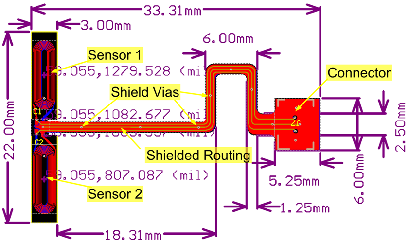 Figure 2-15 Example Dual
Sensor Design
Figure 2-15 Example Dual
Sensor DesignThe stiffeners and spacers are integrated into the sensors for this example. #T4726003-81 shows the arrangement of the spacer and stiffeners.
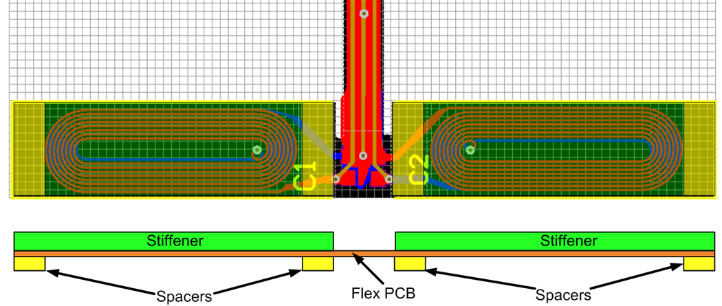 Figure 2-16 Sensor Region
Construction
Figure 2-16 Sensor Region
ConstructionEach sensor region has a dedicated stiffener and two spacers. The flex sensor region between the two sensors provides mechanical isolation between the two sensors.
Table 2-3 shows the sensor stack. The thickness of the stiffener can be varied based on mechanical considerations. In general, incorporating the spacer into the sensor manufacturing can usually provide a tighter tolerance for the spacer thickness than machining the spacer on the case.
| LAYER | TYPE | MATERIAL | THICKNESS (mil) | THICKNESS (mm) | DIELECTRIC MATERIAL |
|---|---|---|---|---|---|
| Stiffener | Dielectric | Core | 32 | 0.813 | FR4 |
| Top Overlay | Overlay | ||||
| Flex Top Coverlay | Solder Mask/Coverlay | Surface Material | 0.4 | 0.010 | Coverlay |
| Top Layer | Signal | Copper | 0.46 | 0.012 | |
| Flex1 | Dielectric | Film | 0.47 | 0.012 | Polyimide |
| Signal Layer | Signal | Copper | 0.46 | 0.012 | |
| Flex2 | Dielectric | Film | 1 | 0.025 | Polyimide |
| Bottom Layer | Signal | Copper | 0.46 | 0.012 | |
| Flex Bottom Coverlay | Solder Mask/Coverlay | Surface Material | 0.4 | 0.010 | Coverlay (PI) |
| Bottom Solder 1 | Solder Mask/Coverlay | Surface Material | 0.4 | 0.010 | Solder Resist |
| Bottom Overlay | Overlay | ||||
| Spacer | Dielectric | Film | 5 | 0.127 | Polyimide |
| Total Thickness | 41.05 | 1.043 |
The spacer and stiffener are only present for a portion of the sensor design, as shown in #T4726003-83. The spacer is only required on the ends of the button locations. The stiffener is required over the sensor and any connectors. The stiffener can be manufactured with a thinner material, if needed for a specific application.
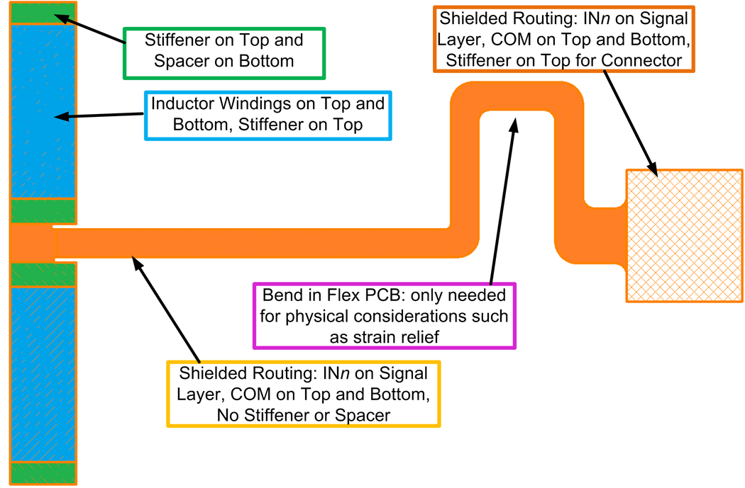 Figure 2-17 Sensor Stack
Across Regions