SSZTC68 september 2015 CSD86350Q5D , LM25145 , LM27402 , LM27403 , LM5145 , LM5175 , LM5175-Q1
As I mentioned in part 1, the printed circuit board (PCB) area dedicated to power management is an immense constraint for system designers. Reducing converter losses is an essential requirement to enable a compact realization in space-constrained applications with limited PCB real estate.
The ability to flexibly deploy a converter at a strategic location on the board is also important – take for instance a high-current point-of-load (POL) module, optimally located adjacent to a load for smaller conduction drop and better load transient performance.
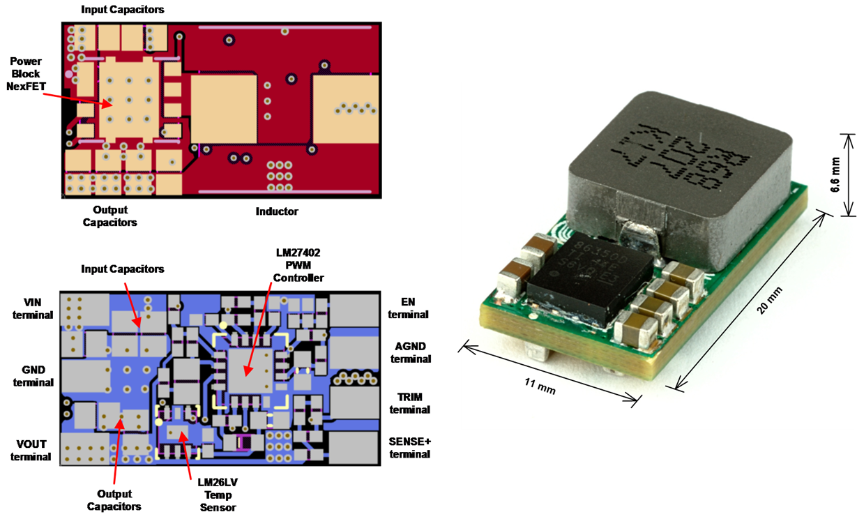
Consider the power stage layout in Figure 1 of a miniaturized form-factor buck converter. As an embedded POL module implementation, it uses an all-ceramic capacitor design, an efficient shielded inductor, vertically stacked MOSFETs, a voltage-mode controller and a six-layer PCB with 2oz copper.
 Figure 1 25A Synchronous Buck Converter
PCB Layout and Implementation.
Figure 1 25A Synchronous Buck Converter
PCB Layout and Implementation.The main tenets of this design are high power density and low bill-of-materials (BOM) cost. It occupies a total PCB area of 2.2cm2 (0.34in2), yielding an effective current density per unit area of 11.3A/cm2 (75A/in2). Power density per unit volume at 3.3V output is 57W/cm3 (930W/in3).
The normal approach to attaining high power density is to increase switching frequency. By contrast, you can achieve miniaturization through strategic component selection while retaining a relatively low switching frequency of 300kHz to lessen frequency proportional losses such as MOSFET switching loss and inductor core loss. Table 1 lists the essential components for this design.
| Power train components | Footprint and profile (mm) | Recommended land pattern outer dimensions (mm) |
|---|---|---|
| CSD86350Q5D NexFETÔ Power Block | 5.0 x 6.0 x 1.5 (SON5x6) | 5.15 x 6.24 |
| LM27402 3V-20V PWM controller | 4.0 x 4.0 x 0.8 (WQFN-16) | 4.2 x 4.2 |
| 0.68µH 1.6mΩ 33A filter inductor | 11.5 x 10.3 x 4.0 | 4.1 x 13.6 |
| 22µF input and 47µF output X5R capacitors | 2.0 x 1.25 x 1.35 (0805) | 2.2 x 1.3 |
| Terminal connections | 2.0 x 3.0 | 2.0 x 3.0 (on host board) |
Value Proposition of High-density PCB Designs
Clearly, the PCB is an important (and sometimes most expensive) component in a design. The value proposition of a well-planned and carefully executed PCB layout for a high-density DC/DC converter lies in:
- More functionality in space-constrained designs (reduced solution volume and footprint).
- Reduced switching-loop parasitic inductance, contributing to:
-
- Lower power MOSFET voltage stress (switch-node voltage spike) and ringing.
- Reduced switching loss.
- Lower electromagnetic interference (EMI), magnetic field coupling and output noise signature.
- Extra margin to survive input rail-transient-voltage disturbances, especially in wide-VIN-range applications.
- Increased reliability and robustness (lower component temperatures).
- Cost savings related to a smaller PCB, fewer filtering components and the elimination of snubbers.
- Differentiated designs provide a competitive advantage, capture customer attention, and increase revenue.
It’s fair to say that PCB layout defines the performance ultimately achieved from a switching power converter. Of course, the designer is quite happy to avoid countless hours of debugging time for EMI, noise, signal integrity, and other issues related to a poor layout.
Additional Resources:
- Read parts 1, 2 and 3 of “DC/DC Converter PCB Layout” on EDN.
- Watch a video on the salient characteristics of high-density buck converter solutions.
- Review the schematic, layout and test reports of these high-density designs from the PowerLabreference design library:
- High-efficiency small form factor 112W sync buck TI Designs reference design.
- High power density voltage regulator module for CPU core power in enterprise switching TI Designs reference design.
- High power density 12Vin, 100W synchronous DC/DC step-down buck converter with inductor-on-top TI Designs reference design.
- Order the high-density LM27403EVM-POL600 30A 600kHz POL evaluation module (EVM).
- Start a design now with WEBENCH® Power Designer.