TIDUF35 june 2023 AM6442
- 1
- Description
- Resources
- Features
- Applications
- 6
- 1System Description
-
2System Overview
- 2.1 Block Diagram
- 2.2 Design Considerations
- 2.3
Highlighted Products
- 2.3.1 AM6442 Microprocessor
- 2.3.2 DP83867 gigabit Ethernet Physical Transceiver
- 2.3.3 DP83TD510E Single-Pair Ethernet Physical Transceiver
- 2.3.4 MSPM0G1107 Microcontroller
- 2.3.5 LMK1C1106 6-Channel Output LVCMOS 1.8-V Buffer
- 2.3.6 LMK6C Low-Jitter, High-Performance, Bulk-Acoustic-Wave (BAW) Fixed-Frequency LVCMOS Oscillator
- 2.3.7 TLVM13630 High-Density, 3-V to 36-V Input, 1-V to 6-V Output, 3-A Step-Down Power Module
- 2.3.8 LM74700-Q1 Reverse-Polarity Protection Ideal Diode
- 2.3.9 TPS62825A Synchronous Step-Down DC-DC Converter
- 2.3.10 LMR36006 Ultra-Small Synchronous Step-Down Converter
- 2.3.11 TLV62568A High-Efficiency Step-Down Buck Converter With Forced PWM
- 3System Design Theory
- 4Hardware, Software, Testing Requirements, and Test Results
- 5Design and Documentation Support
- 6About the Author
4.1.1 Board Interface
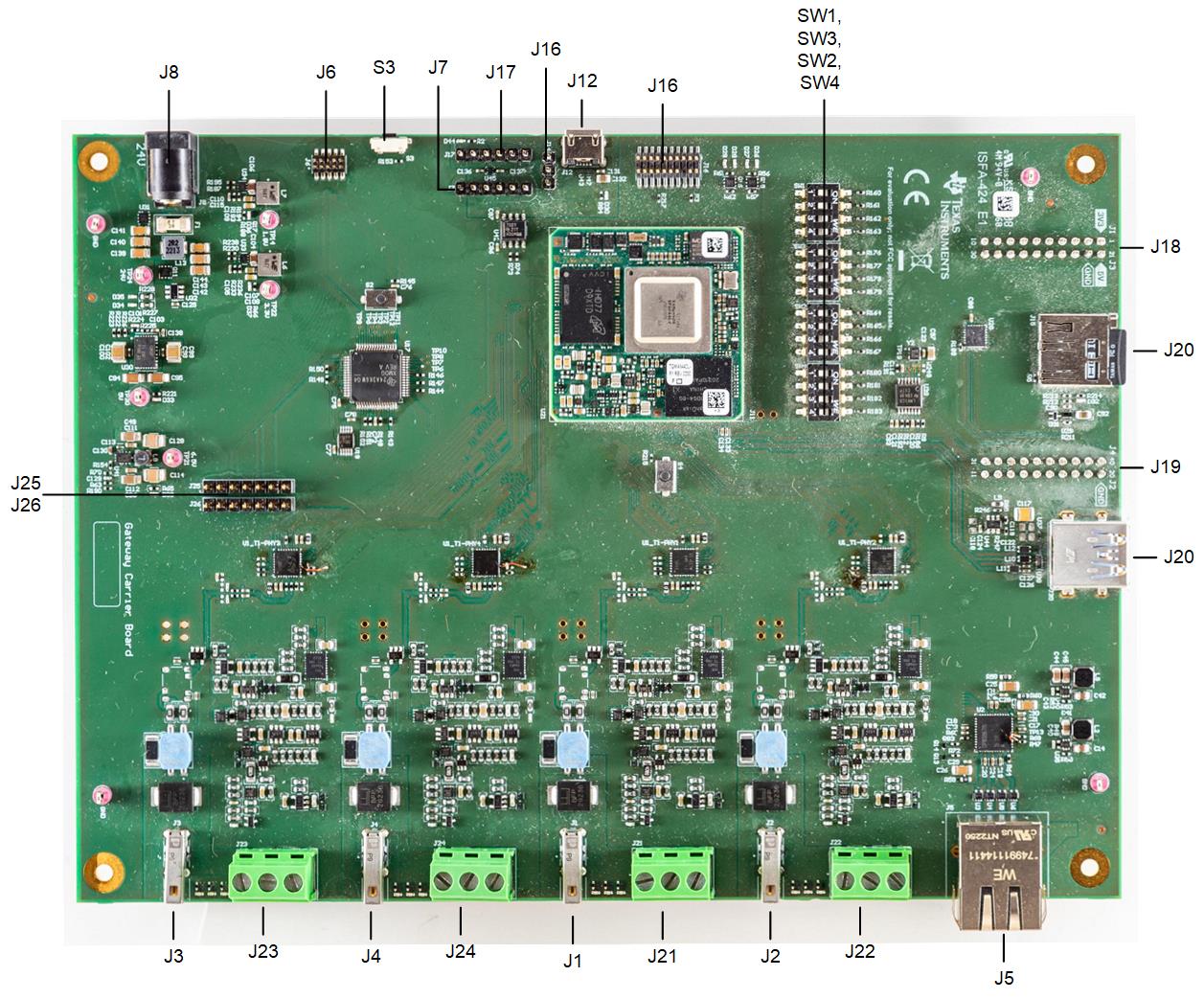
Figure 4-1 shows various connectors, switches, and jumpers used to interface with the reference design.
 Figure 4-1 Interfaces on Gateway
Board
Figure 4-1 Interfaces on Gateway
BoardTable 4-1 Board Connectors, Switches,
and Headers
| CONNECTOR | DESCRIPTION |
|---|---|
| J8 | External 24-V supply |
| J6 | JTAG interface MSPM0 |
| S3 | RESET button MSPM0 |
| J17 | UART0 TXD, RXD interface of AM6442 |
| J7 | UART TXD, RXD interface of MSPM0 |
| J14 | Power supply selector for ISO7021 - set jumper to 1-2 for selecting power from FTDI device. Refer to schematic. |
| J12 | Micro USB interface to UART0 serial console terminal of AM6442 |
| SW1, SW2, SW3, SW4 | AM6442 boot mode switches |
| J18, J19 | Interface to CC3301 Wi-Fi and Bluetooth® BoosterPack Plug-in Module (BP-CC3301) |
| J20 | USB 3 Type A connector |
| J15 | μSD card slot |
| J5 | Gigabit RJ45 connector |
| J16 | JTAG interface AM6442 |
| S4 | RESET button AM6442 |
| J1, J21 | Single pair Ethernet connector port 1 |
| J2, J22 | Single pair Ethernet connector port 2 |
| J3, J23 | Single pair Ethernet connector port 3 |
| J4, J24 | Single pair Ethernet connector port 4 |
| J25, J26 | PoDL debug interface for single pair Ethernet port 3 |