TIDUF63 December 2023
- 1
- Description
- Resources
- Features
- Applications
- 6
- 1System Description
- 2System Design Theory
-
3System Overview
- 3.1 Block Diagram
- 3.2 Design Considerations
- 3.3
Highlighted Products
- 3.3.1 TMDSCNCD280039C - TMS320F280039C Evaluation Module C2000™ MCU controlCARD™
- 3.3.2 LMG3522R050 - 650-V 50-mΩ GaN FET With Integrated Driver
- 3.3.3 LMG2100R044 - 100-V, 35-A GaN Half-Bridge Power Stage
- 3.3.4 TMCS1123 - Precision Hall-Effect Current Sensor
- 3.3.5 AMC1302 - Precision, ±50-mV Input, Reinforced Isolated Amplifier
- 3.3.6 AMC3330 - Precision, ±1-V Input, Reinforced Isolated Amplifier With Integrated DC/DC Converter
- 3.3.7 AMC1311 - High-Impedance, 2-V Input, Reinforced Isolated Amplifier
- 3.3.8 ISO6741 - General-Purpose Reinforced Quad-Channel Digital Isolators with Robust EMC
- 3.3.9 UCC21540 - Reinforced Isolation Dual-Channel Gate Driver
- 3.3.10 LM5164 - 100-V Input, 1-A Synchronous Buck DC/DC Converter with Ultra-low IQ
- 4Hardware, Software, Testing Requirements, and Test Results
- 5Design and Documentation Support
- 6About the Author
2.1 Boost Converter Design
The inductor is the most important component in power regulator design. There are three important inductor specifications: inductor value, saturation current, and DC resistance (DCR).
In a boost regulator, the inductor DC current can be calculated by Equation 1.
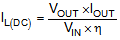
where
- VOUT is the output voltage of the boost converter
- IOUT is the output current of the boost converter
- VIN is the input voltage of the boost converter
- η is the power conversion efficiency, use 90% for most applications
The inductor ripple current is calculated using Equation 2.
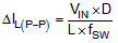
where
- D is the duty cycle
- L is the inductance value of the inductor
- fSW is the switching frequency
- VIN is the input voltage of the boost converter
Therefore, the inductor peak current is calculated with Equation 3.
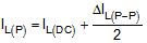
Normally, it is advisable to work with an inductor peak-to-peak current of less than 40% of the average inductor current for maximum output current. A smaller ripple from a larger valued inductor reduces the magnetic hysteresis losses in the inductor and EMI. But in the same way, load transient response time is increased. The saturation current of the inductor must be higher than the calculated peak inductor current.