SNVSA18C April 2014 – August 2014 ADC16DX370
PRODUCTION DATA.
- 1 Features
- 2 Applications
- 3 Description
- 4 Revision History
- 5 Pin Configuration and Functions
-
6 Specifications
- 6.1 Absolute Maximum Ratings
- 6.2 Handling Ratings
- 6.3 Recommended Operating Conditions
- 6.4 Thermal Information
- 6.5 Converter Performance Characteristics
- 6.6 Power Supply Electrical Characteristics
- 6.7 Analog Interface Electrical Characteristics
- 6.8 CLKIN, SYSREF, SYNCb Interface Electrical Characteristics
- 6.9 Serial Data Output Interface Electrical Characteristics
- 6.10 Digital Input Electrical Interface Characteristics
- 6.11 Timing Requirements
- 6.12 Typical Characteristics
- 7 Parameter Measurement Information
-
8 Detailed Description
- 8.1 Overview
- 8.2 Functional Block Diagram
- 8.3
Feature Description
- 8.3.1 Amplitude and Phase Imbalance Correction of Differential Analog Input
- 8.3.2 DC Offset Correction
- 8.3.3 Over-Range Detection
- 8.3.4 Input Clock Divider
- 8.3.5 SYSREF Offset Feature and Detection Gate
- 8.3.6 Sampling Instant Phase Adjustment
- 8.3.7 Serial Differential Output Drivers
- 8.3.8 ADC Core Calibration
- 8.3.9 Data Format
- 8.3.10 JESD204B Supported Features
- 8.3.11 Transport Layer Configuration
- 8.3.12 Test Pattern Sequences
- 8.3.13 JESD204B Link Initialization
- 8.3.14 SPI
- 8.4 Device Functional Modes
- 8.5 Register Map
- 9 Application and Implementation
- 10Power Supply Recommendations
- 11Layout
- 12Device and Documentation Support
- 13Mechanical, Packaging, and Orderable Information
Package Options
Mechanical Data (Package|Pins)
- RME|56
Thermal pad, mechanical data (Package|Pins)
Orderable Information
9 Application and Implementation
9.1 Application Information
9.1.1 Analog Input Considerations
9.1.1.1 Differential Analog Inputs and Full Scale Range
The ADC16DX370 device has two channels, each with a pair of analog signal input pins: VINA+, VINA− for channel A and VINB+, VINB− for channel B. VIN, the input differential signal for a channel, is defined as VIN = (VIN+) – (VIN−). Table 28 shows the expected input signal range when the differential signal swings about the input common mode, VCM. The full-scale differential peak-to-peak input range is equal to twice the internal reference voltage, VREF. Nominally, the full scale range is 1.7 Vpp-diff, therefore the maximum peak-to-peak single-ended voltage is 0.85 Vpp at each of the VIN+ and VIN− pins.
The single-ended signals must be opposite in polarity relative to the VCM voltage to provide a purely differential signal, otherwise the common-mode component may be rejected by the ADC input. Table 28 indicates the input to output relationship of the ADC16DX370 device where VREF = 0.85 V. Differential signals with amplitude or phase imbalances result in lower system performance compared to perfectly balanced signals. Imbalances in signal path circuits lead to differential-to-common-mode signal conversion and differential signal amplitude loss as shown in Figure 37. This deviation or imbalance directly causes a reduction in the signal amplitude and may also lead to distortion, particularly even order harmonic distortion, as the signal propagates through the signal path. The differential imbalance correction feature of the ADC16DX370 device helps to correct amplitude or phase errors in the signal.
Table 28. Mapping of the Analog Input Full Scale Range to Digital Codes
| VIN+ | VIN– | 2s Complement Output | Binary Output | Note |
|---|---|---|---|---|
| VCM – VREF / 2 | VCM + VREF / 2 | 1000 0000 0000 0000 | 0000 0000 0000 0000 | Negative full-scale |
| VCM – VREF / 4 | VCM + VREF / 4 | 1100 0000 0000 0000 | 0100 0000 0000 0000 | |
| VCM | VCM | 0000 0000 0000 0000 | 1000 0000 0000 0000 | Mid-scale |
| VCM + VREF / 4 | VCM – VREF / 4 | 0100 0000 0000 0000 | 1100 0000 0000 0000 | |
| VCM + VREF / 2 | VCM – VREF / 2 | 0111 1111 1111 1111 | 1111 1111 1111 1111 | Positive full-scale |
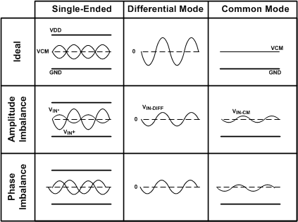 Figure 37. Differential Signal Waveform and Signal Imbalance
9.1.1.2 Analog Input Network Model
Matching the impedance of the driving circuit to the input impedance of the ADC can be important for low distortion performance and a flat gain response through the network across frequency. In very broadband applications or lowpass applications, the ADC driving network must have very low impedance with a small termination resistor at the ADC input to maximize the bandwidth and minimize the bandwidth limitation posed by the capacitive load of the ADC input. In bandpass applications, a designer may either design the anti-aliasing filter to match to the complex impedance of the ADC input at the desired intermediate frequency, or consider the resistive part of the ADC input to be part of the resistive termination of the filter and the capacitive part of the ADC input to be part of the filter itself. The capacitive load of the ADC input can be easily absorbed into most LC bandpass filter designs with a final shunt LC tank stage.
The analog input circuit of the ADC16DX370 device is a buffered input with an internal differential termination. Compared to an ADC with a switched-capacitor input sampling network that has an input impedance that varies with time, the ADC16DX370 device provides a constant input impedance that simplifies the interface design joining the ADC and ADC driver. A simplified passive model of the ADC input network is shown in Figure 38 that includes the termination resistance, input capacitance, parasitic bond-wire inductance, and routing parastics.
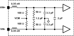 Figure 38. Simplified Analog Input Network Circuit Model
A more accurate load model is described by the measured differential SDD11 (100-Ω) parameter model. A plot of the differential impedance derived from the model is shown on the Smith chart of Figure 39. The model includes the internal 200-Ω resistive termination, the capacitive loading of the input buffer, and stray parasitic impedances like bond wire inductance and signal routing coupling. The S11_diff model may be used to back-calculate the impedance of the ADC input at a frequency of interest.
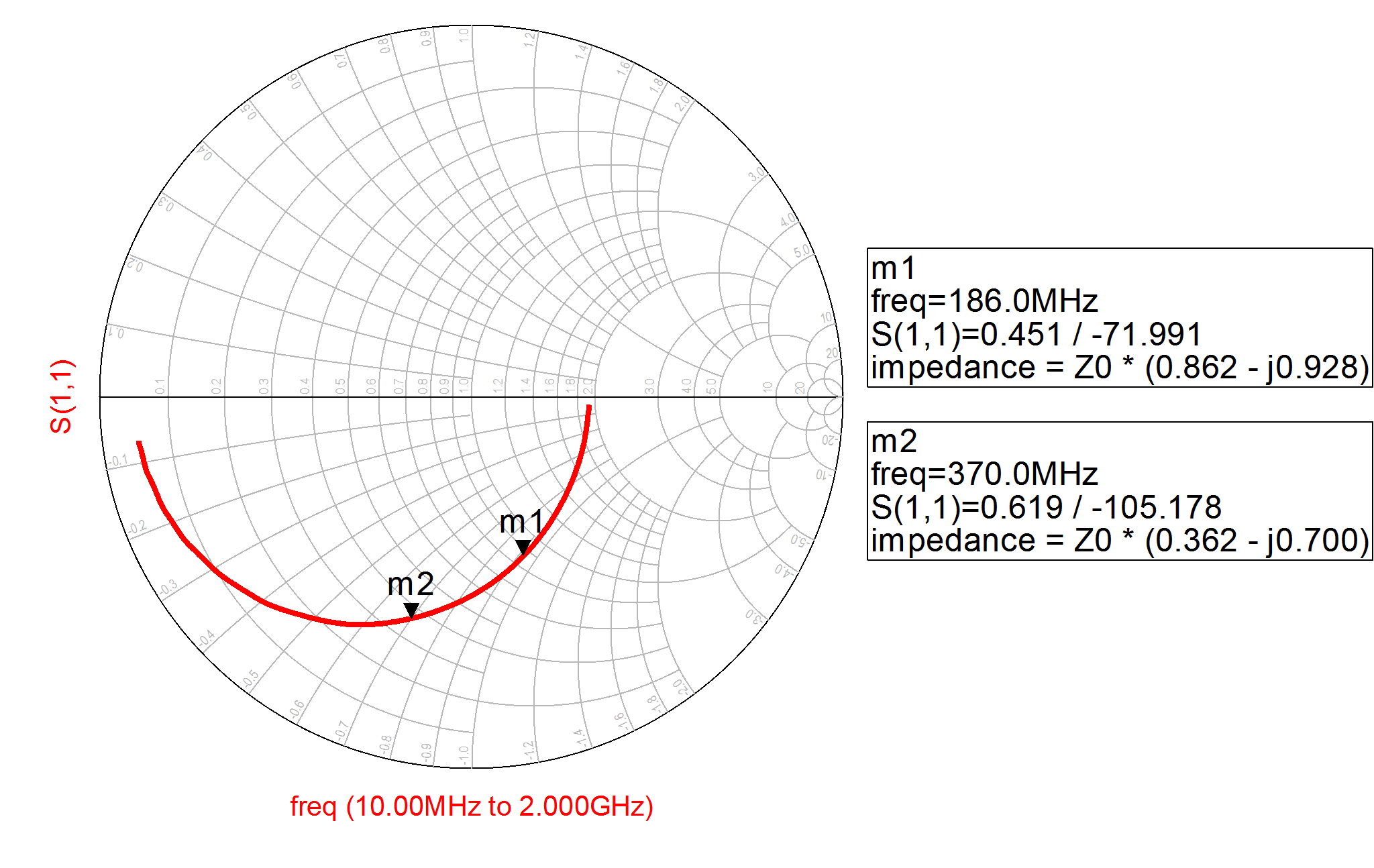 Figure 39. Measured Differential Impedance of Analog Input Network on a Smith Chart (100 Ω)
9.1.1.3 Input Bandwidth
The input bandwidth of the ADC16DX370 device is defined here as the frequency at which the fundamental amplitude of the sampled data deviates by 3 dB, compared to the amplitude at low frequencies, for a low-impedance input sinusoidal signal with constant voltage amplitude at the VIN+ and VIN– input pins. The voltage frequency response is shown in Figure 40.
The peaking in the frequency response is caused by the resonance between the package bond wires and input capacitance as well as a parasitic 0.5-nH series trace inductance leading to the device pins. This peaking is typically made insignificant by the stop-band of an anti-aliasing filter that precedes the ADC input. For broadband applications, 10-Ω resistors may be put in series with the VIN+ and VIN– input pins. This extra resistance flattens out the frequency response at the cost of adding some attenuation in the signal path. The additional series resistance also accordingly modifies the measured SDD11 looking into the analog input.
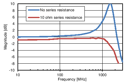 Figure 40. Measured Input Voltage Frequency Response
9.1.1.4 Driving the Analog Input
The ADC16DX370 device analog input may be driven by a number of methods depending on the end application. The most important design aspects to consider when designing the ADC voltage driver network are signal coupling, impedance matching, differential signal balance, anti-alias filtering, and signal level.
An analog signal is AC or DC coupled to the ADC depending on whether signal frequencies near DC must be sampled. DC coupling requires tight control of the output common-mode of the ADC driver to match the input common-mode of the ADC input. In the case of DC coupling, the biases at pins VCMA and VCMB may be used as references to establish the driver output common-mode, but the load cannot source or sink more current than what is specified in the electrical parameters. AC coupling does not require strict common-mode control of the driver and is typically achieved using AC coupling capacitors or a flux-coupled transformer. AC coupling capacitors should be chosen to have 0.1-Ω impedance or less over the frequency band of interest. LC filter designs may be customized to achieve either AC or DC coupling.
The internal input network of the ADC16DX370 device has the common-mode voltage bias provided through internal shunt termination resistors, as shown in Figure 38. TI also recommends providing the common-mode reference externally from the VCMA and VCMB pins, through external termination resistors. VCMA is used exclusively for channel A and is independent from VCMB.
Impedance matching in high speed signal paths using an ADC is dictated by the characteristic impedance of interconnects and by the design of anti-aliasing filters. Matching the source to the load termination is critical to ensure maximum power transfer to the load and to maintain gain flatness across the desired frequency band. In applications with signal transmission lengths greater than 10% of the smallest signal wavelength (0.1 λ), matching is also desirable to avoid signal reflections and other transmission line effects. Applications that require high order anti-aliasing filters designs, including LC bandpass filters, require an expected source and load termination to guarantee the passband bandwidth and ripple of the filter design. The recommended range of the ADC driver source termination and ADC load termination is from 50- to 200-Ω differential. The ADC16DX370 device has an internal differential load termination, but additional termination resistance may be added at the ADC input pins to adjust the total termination. The load termination at the ADC input presents a system-level design tradeoff. Better 2nd order distortion performance (HD2, IMD2) is achieved by the ADC using a lower load termination resistance, but the ADC driver must have a higher drive strength and linearity to drive the lower impedance. Choosing a 100-Ω total load termination is a reasonable balance between these opposing requirements.
Differential signal balance is important to achieve high distortion performance, particularly even order distortion (HD2, HD4). Circuits such as transformers and filters in the signal path between the signal source and ADC can disrupt the amplitude and phase balance of the differential signal before reaching the ADC input due to component tolerances or parasitic mismatches between the two parallel paths of the differential signal. The amplitude mismatch in the differential path should be less than ± 0.4 dB and the phase mismatch should be less than ± 2° to achieve a high level of HD2 performance. In the case that this imbalance is exceeded, the input balance correction may be used to re-balance the signal and improve the performance. Driving the ADC16DX370 device with a single-ended signal is not supported due to the tight restriction on the ADC input common-mode to maintain good distortion performance.
Converting a single-ended signal to a differential signal may be performed by an ADC driver or transformer. The advantages of the ADC driver over a transformer include configurable gain, isolation from previous stages of analog signal processing, and superior differential signal balancing. The advantages of using a transformer include no additional power consumption and little additional noise or distortion.
Figure 41 is an example of driving the ADC input with a cascaded transformer configuration. The cascaded transformer configuration provides a high degree of differential signal balancing, the series 0.1-µF capacitors provide AC coupling, and the additional 33-Ω termination resistors provide a total differential load termination of 50 Ω. When additional termination resistors are added to change the ADC load termination, shunt terminations to the VCM reference are recommended to reduce common-mode fluctuations or sources of common-mode interference. A differential termination may be used if these sources of common-mode interference are minimal. In either case, the additional termination components must be placed as close to the ADC pins as possible. The MABA007159 transmission-line transformer from this example is widely available and results in good differential balance, although improved balance may be achieved using the rarer MABACT0040 transformer. Shunt capacitors at the ADC input, used to suppress the charge kickback of an ADC with switched-capacitor inputs, are not required for this purpose because the buffered input of the ADC16DX370 device does not kickback a significant amount of charge.
The insertion loss between an ADC driver and the ADC input is important because the driver must overcome the insertion loss of the connecting network to drive the ADC to full-scale and achieve the best SNR. Minimizing the loss through the network reduces the output swing and distortion requirements of the driver and usually translates to a system-level power savings in the driver. This can be accomplished by selecting transformers or filter designs with low insertion loss. Some filter designs may employ reduced source terminations or impedance conversions to minimize loss. Many designs require the use of high-Q inductors and capacitors to achieve an expected passband flatness and profile.
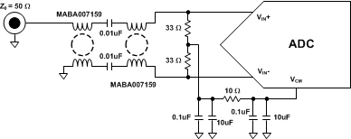 Figure 41. Transformer Input Network
Sampling theory states that if a signal with frequency ƒIN is sampled at a rate less than 2 × ƒIN, then it experiences aliasing, causing the signal to fall at a new frequency between 0 and FS / 2 and become indistinguishable from other signals at that new frequency.
To prevent out-of-band interference from aliasing onto a desired signal at a particular frequency, an anti-aliasing filter is required at the ADC input to attenuate the interference to a level below the level of the desired signal. This is accomplished by a lowpass filter in systems with desired signals from DC to FS / 2 or with a bandpass filter in systems with desired signals greater than FS / 2 (under-sampled signals). If an appropriate anti-aliasing filter is not included in the system design, the system may suffer from reduced dynamic range due to additional noise and distortion that aliases into the frequency bandwidth of interest.
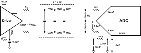
An anti-aliasing filter is required in front of the ADC input in most applications to attenuate noise and distortion at frequencies that alias into any important frequency band of interest during the sampling process. An anti-aliasing filter is typically a LC lowpass or bandpass filter with low insertion loss. The bandwidth of the filter is typically designed to be less than FS / 2 to allow room for the filter transition band. Figure 42 is an example architecture of a 9 pole order LC bandpass anti-aliasing filter with added transmission zeros that can achieve a tight filtering profile for second Nyquist zone under-sampling applications.
Maximizing the distortion performance of this device requires the avoidance of driving circuits that are mostly capacitive at frequencies near and above the sampling rate. At these frequencies, the performance is maximized by ensuring the driving circuit is high impedance or mostly resistive (real impedance). Driving circuits with highly capacitive sources impedances (negative source reactance) at these frequencies can cause resonance with the interface, leading to sub-optimal distortion performance. In the case of bandpass LC anti-aliasing filters, the impedance looking into the filter output is recommended to be high impedance or real at frequencies near and above the sampling rate such as the filter shown in Figure 42. Capacitors placed directly at the ADC input used as bandwidth limiters or as part of a filter's final stage LC tank are not recommended.
Applications that use lumped reactive components (capacitors, inductors) in the interface to the ADC are recommended to have a small series resistor at the ADC input, also shown in Figure 42. Place these resistors close to the device pins, between the external termination resistors and the device pins. A value of 5 Ω is sufficient for most applications, though TI recommends 10 Ω for applications where the lumped differential capacitance at the ADC input is unavoidable and greater than 2 pF.
DC coupling to the analog input is also possible but the input common-mode must be tightly controlled for guaranteed performance. The driver device must have an output common-mode that matches the input common-mode of the ADC16DX370 device and the driver must track the VCM output from the ADC16DX370 device, as shown in the example DC coupled interface of Figure 43 because the input common-mode varies with temperature. The common-mode path from the VCM output, through the driver device, back to the ADC16DX370 device input, and through a common-mode detector inside the ADC16DX370 device forms a closed tracking loop that will correct common-mode offset contributed by the driver device but the loop must be stable to ensure correct performance. The loop requires the large, 10-µF capacitor at the VCM output to establish the dominant pole for stability and the driver device must reliably track the VCM output voltage bias. The current drive strength and voltage swing of the VCM output bias limits the correctable amount of common-mode offset.
9.1.1.5 Clipping and Over-Range
The ADC16DX370 device has two regions of signal clipping: code clipping (over-range) and ESD clipping. When the input signal amplitude exceeds the full-scale reference range, code clipping occurs during which the digital output codes saturate. If the signal amplitude increases beyond the absolute maximum rating of the analog inputs, ESD clipping occurs due to the activation of ESD diodes.
The thresholds of the indicators are programmable via the SPI. An over-range hold feature is also available to extend the time duration of the indicator longer than the over-range event itself to accommodate the case that a device monitoring the OVRA and OVRB outputs cannot process at the rate of the ADC sampling clock.
TI does not recommend ESD clipping and activation of the ESD diodes at the analog input, which may damage or shorten the life of the device. This clipping may be avoided by selecting an ADC driver with an appropriate saturating output voltage, by placing insertion loss between the driver and ADC, by limiting the maximum amplitude earlier in the signal path at the system level, or by using a dedicated differential signal limiting device such as back-to-back diodes. Any signal swing limiting device must be chosen carefully to prevent added distortion to the signal.
9.1.2 CLKIN, SYSREF, and SYNCb Input Considerations
Clocking the ADC16DX370 device shares many common concepts and system design requirements with previously released ADC products, but the JESD204B supported architecture adds another layer of complexity to clocking at the system level. A SYSREF signal accompanies the device clock to provide phase alignment information for the output data serializer (as well as for the sampling instant when the clock divider is enabled) to ensure that the latency through the JESD204B link is always known and does not vary, a concept called deterministic latency. To ensure deterministic latency, the SYSREF signal must meet setup and hold requirements relative to CLKIN and the design of the clocking interfaces require close attention. As with other ADCs, the quality of the clock signal also influences the noise and spurious performance of the device.
9.1.2.1 Driving the CLKIN+ and CLKIN– Input
The CLKIN input circuit is composed of a differential receiver and an internal 100-Ω termination to a weakly driven common-mode of 0.55 V. TI recommends AC coupling to the CLKIN input with 0.1-uF external capacitors to maintain the optimal common-mode biasing. Figure 44 shows the CLKIN receiver circuit and an example AC coupled interface.
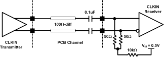 Figure 44. Driving the CLKIN Input With an AC Coupled Interface
DC coupling is allowed as long as the input common-mode range requirements are satisfied. The input common-mode of the CLKIN input is not compatible with many common signaling standards like LVDS and LVPECL. Therefore, the CLKIN signal driver common-mode must be customized at the transmitter or adjusted along the interface. Figure 45 shows an example DC coupled interface that uses a resistor divider network to reduce the common-mode while maintaining a 100-Ω total termination at the load. Design equations are provided with example values to determine the resistor values.
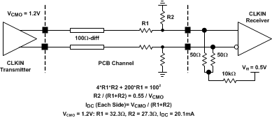 Figure 45. Driving the CLKIN Input With an Example DC Coupled Interface
The CLKIN input supports any type of standard signaling that meets the input signal swing and common-mode range requirements with an appropriate interface. Generic differential sinusoidal or square-wave clock signals are also supported. TI does not recommend driving the CLKIN input single-ended. The differential lane trace on the PCB should be designed to be a controlled 100 Ω and protected from noise sources or other signals.
9.1.2.2 Clock Noise and Edge Rate
Noise added to the sampling clock path of the ADC degrades the SNR performance of the system. This noise may include broadband noise added by the ADC clock receiver inside the ADC device but may also include broadband and in-close phase noise added by the clock generator and any other devices leading to the CLKIN input. The theoretical SNR performance limit of the ADC16DX370 device as a result of clock noise for a given input frequency is shown in Figure 46 for a full scale input signal and different values of total jitter.
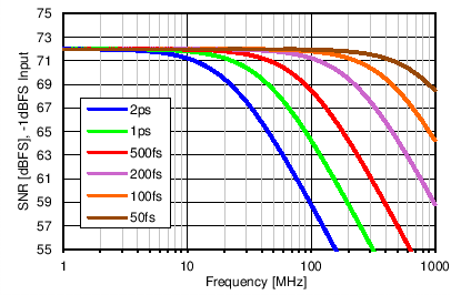 Figure 46. SNR Limit Due to Jitter of Sampling Clock With a Full-Scale Input Signal
The differential clock receiver of the ADC16DX370 device has a very-low noise floor and wide bandwidth. The wide band clock noise of the receiver, also referred to as the additive jitter, modulates the sampling instant and adds the noise to the signal. At the sampling instant, the added broadband noise appears in the first Nyquist zone at the ADC output to degrade the noise performance. Minimizing the additive jitter requires a sampling clock with a steep edge rate at the zero crossing. Reduced edge rate increases the additive jitter. For clock signals with a differential swing of 100 mV or greater, the additive clock Figure 47 shows the SNR performance (integrated within a 100-MHz bandwidth) of the ADC16DX370 device for a range of clock transition slopes.
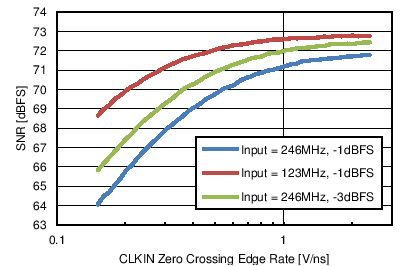 Figure 47. SNR (in 100-MHz Bandwidth) vs Input Clock Edge Rate
Noise added to the sampling clock by devices leading up to the ADC clock input also directly affects the noise performance of the system. In-close phase noise is typically dominated by the performance of the clock reference and phase-locked loop (PLL) that generates the clock and limits the sensitivity of the sampling system at desired frequencies offset 100 Hz to 10 MHz away from a large blocking signal. Little can be done to improve the in-close phase noise performance without the use of an additional PLL. Broadband noise added in the clock path limits the sensitivity of the whole spectrum and may be improved by using lower noise devices or by inserting a band-pass filter (BPF) with a narrow pass band and low insertion loss to the clock input signal path. Adding a BPF limits the transition rate of the clock, thereby creating a trade-off between the additive jitter added by the ADC clock receiver and the broadband noise added by the devices that drive the clock input.
Additional noise may couple to the clock path through power supplies. Take care to provide a very-low noise power supply and isolated supply return path to minimize noise added to the supply. Spurious noise added to the clock path results in symmetrical, modulated spurs around large input signals. These spurs have a constant magnitude in units of dB relative to the input signal amplitude or carrier, [dBc].
9.1.2.3 Driving the SYSREF Input
The SYSREF input interface circuit is composed of the differential receiver, internal common-mode bias, SYSREF offset feature, and SYSREF detection feature.
A high impedance (10-kΩ) reference biases the input common-mode through internal 1-kΩ termination resistors. The bias voltage is similar to the CLKIN input common-mode bias, but the internal differential termination is different. The SYSREF input requires an external 100-Ω termination. A network of resistors and switches are included at the input interface to provide a programmable DC offset, referred to as the SYSREF offset feature. This feature is configurable through the SPI and may be used to force a voltage offset at the SYSREF input in the absence of an active SYSREF signal. Following the receiver, an AND gate provides a method for detecting or ignoring incoming SYSREF events.
The timing relationship between the CLKIN and SYSREF signal is very stringent in a JESD204B system. Therefore, the signal path network of the CLKIN and SYSREF signals must be as similar as possible to ensure that the signal relationship is maintained from the launch of the signal, through their respective channels to the CLKIN and SYSREF input receivers.
TI recommends AC coupling for the SYSREF interface as shown in Figure 48. This network closely resembles the AC coupled interface of the CLKIN input shown in Figure 44 with the exception of the 100-Ω termination resistor on the source side of the AC coupling capacitors. This resistor is intentionally placed on the source side of the AC coupling capacitors, so that the termination does not interfere with the DC biasing capabilities of the SYSREF offset feature. In the case of AC coupling, the coupling capacitors of both the CLKIN and SYSREF interfaces, as well as the SYSREF termination resistor, must be placed as close as possible to the pins of the ADC16DX370 device.
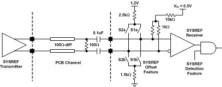 Figure 48. SYSREF Input Receiver and AC Coupled Interface
DC coupling of the SYSREF interface is possible, but not recommended. DC coupling allows all possible SYSREF signaling types to be used without the use of the SYSREF offset feature, but it has strict common-mode range requirements. The example DC coupled configuration of Figure 49 uses the same technique for the CLKIN example DC coupled interface and also includes the 100-Ω external termination. A drawback of the example DC coupled interface is that the resistor divider draws a constant DC current that must be sourced by the SYSREF transmitter.
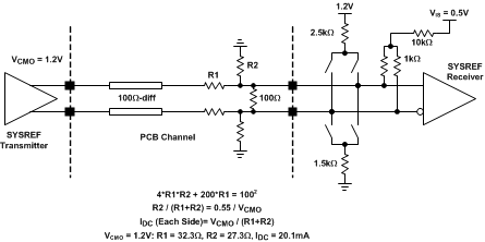 Figure 49. Example DC Coupling to the SYSREF Input
9.1.2.4 SYSREF Signaling
The SYSREF input may be driven by a number of different types of signals. The supported signal types, shown in Figure 50 (in single-ended form), include periodic, gapped periodic, and one-shot signals. The rising edge of the SYSREF signal is used as a reference to align the internal frame clock and local multi-frame clock (LMFC). To ensure proper alignment of these system clocks, the SYSREF signal must be generated along with the CLKIN signal such that the SYSREF rising edge meets the setup and hold requirements relative to the CLKIN at the ADC16DX370 device inputs.
For each rising clock edge that is detected at the SYSREF input, the ADC16DX370 device compares the current alignment of the internal frame and LMFC with the SYSREF edge and determines if the internal clocks must be re-aligned. In the case that no alignment is needed, the clocks maintain their current alignment and the JESD204B data link is not broken. In the case that re-alignment is needed, the JESD204B data link is broken and the clocks are re-aligned.
 Figure 50. SYSREF Signal Types (Single-Ended Representations)
In the case of a periodic SYSREF signal, the frame and LMFC alignment is established at the first rising edge of SYSREF, and every subsequent rising edge (that properly meets setup and hold requirements) is ignored because the alignment has already been established. A periodic SYSREF must have a period equal to n × K / FS where ‘FS’ is the sampling rate, ‘K’ is the JESD204B configuration parameter indicating the number of frames per multi-frame, and ‘n’ is an integer of one or greater. The duty cycle of the SYSREF signal should be greater than 2 / K but less than (K – 2) / K.
Gapped-period signals contain bursts of pulses. The frame and LMFC alignments are established on the first rising edge of the pulse burst. The rising edges within the pulse burst must be spaced apart by n × K / FS seconds, similar to the periodic SYSREF signal. Any rising edge that does not abide by this rule or does not meet the setup and hold requirements forces re-alignment of the clocks. The duty cycle requirements are the same as the periodic signal type.
A one-shot signal contains a single rising edge that establishes the frame and LMFC alignment. The single pulse duration must be 2 × TFRAME or greater.
TI recommends gapped-periodic or one-shot signals for most applications because the SYSREF signal is not active during normal sampling operation. Periodic signals that toggle constantly introduce spurs into the signal spectrum that degrade the sensitivity of the system.
9.1.2.5 SYSREF Timing
The SYSREF timing requirements depend on whether deterministic latency of the JESD204B link is required.
If deterministic latency is required, then the SYSREF signal must meet setup and hold requirements relative to the CLKIN signal. In the case that the internal CLKIN divider is used and a very high-speed signal is provided to the CLKIN input, the SYSREF signal must meet setup and hold requirements relative to the very high-speed signal at the CLKIN input.
If deterministic latency is not required, then the SYSREF signal may be supplied as an asynchronous signal (possibly achieving < ± 2 frame clock cycles latency variation) or not provided at all (resulting in latency variation as large as the multi-frame period).
9.1.2.6 Effectively Using the SYSREF Offset and Detection Gate Features
Selecting the proper settings for the SYSREF offset feature depends on the condition of SYSREF in the idle state and the type of SYSREF signal being transmitted. Table 29 describes the possible SYSREF idle cases and the corresponding SYSREF offset to apply.
TI recommends the use of the SYSREF detection gate for most applications. The gate is enabled when SYSREF is being transmitted and the gate is disabled before the SYSREF transmitter is put in the idle state. Although the SYSREF offset feature does not support situations where the SYSREF transmitter is in a 0 V or Hi-Z common-mode condition during the idle state, the SYSREF gate can be used to ignore the SYSREF input during those conditions. In those cases, time is required to dissipate the voltage build-up on the AC coupling capacitors when the SYSREF returns to an active state.
Enabling the SYSREF gate immediately sends a logic signal to a logic block responsible for aligning the internal frame clock and LMFC. If the signal at the SYSREF input is logic high when the gate is enabled, then a "false" rising edge event causes a re-alignment of the internal clocks, despite the fact that the event is not an actual SYSREF rising edge. The SYSREF rising edge following the gate enable then causes a subsequent re-alignment with the desired alignment.
TI highly recommends the SYSREF clocking schemes described in Table 30.
Table 29. SYSREF Offset Feature Usage Cases
| SYSREF Signal Type |
SYSREF Idle VOD at TX |
SYSREF Idle Common-Mode (VIS) at the Transmitter | SYSREF Offset Feature Setting |
|---|---|---|---|
| Periodic | N/A | N/A | 0 mV |
| Gapped-periodic or One-shot |
= 0 | VIS same during idle and non-idle states | 0 mV |
| > 0 (logic high) | VIS same during idle and non-idle states | 400 mV | |
| < 0 (logic low) | VIS same during idle and non-idle states | –400 mV | |
| Any | 0 | 0 | SYSREF offset feature does not support these cases |
| Hi-Z | Hi-Z |
Table 30. Recommended SYSREF Clocking Schemes
| Coupling | SYSREF Type | SYSREF at TX During Idle State | SYSREF Rx Offset Setting | SYSREF Detection Gate |
|---|---|---|---|---|
| AC Coupled | One-shot or gapped-periodic(1) | VOD logic low, VIS does not change during idle | –400 mV at all times | Disabled during SYSREF idle, enabled during LMFC alignment |
| DC Coupled | One-shot or gapped-periodic | VOD either logic state, VIS does not change during idle | 0 mV at all times | Disabled during SYSREF idle, enabled during LMFC alignment |
9.1.2.7 Driving the SYNCb Input
The SYNCb input is part of the JESD204B interface and is used to send synchronization requests from the serial data receiver to the transmitter, the ADC16DX370 device. The SYNCb signal, quantified as the (SYNCb+ – SYNCb–), is a differential active low signal. In the case of the ADC16DX370 device, a JESD204B subclass 1 device, a SYNCb assertion (logic low) indicates a request for synchronization by the receiver.
The SYNCb input is a differential receiver as shown in Figure 51. Resistors provide an internal 100-Ω differential termination as well as a voltage divider circuit that gives the SYNCb receiver a wide input common-mode range. The SYNCb signal must be DC coupled from the driver to the SYNCb inputs; therefore, the wide common-mode range allows the use of many different logic standards including LVDS and LVPECL. No additional external components are needed for the SYNCb signal path as shown in the interface circuit of Figure 51, but providing an electrical probing site is recommended for system debug.
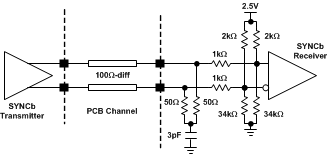 Figure 51. SYNCb Input Receiver and Interface
The SYNCb input is an asynchronous input and does not have sub-clock-cycle setup and hold requirements relative to the CLKIN or any other input to the ADC16DX370 device. The SYNCb input also does not have setup and hold requirements relative to the frame and LMFC system clocks unless the delay through the JESD204B link is longer than a multi-frame. A design that has link delay greater than a multi-frame does not strictly follow the standard rules for achieving deterministic latency, but may be required in many applications and may still achieve deterministic latency. In this case, it is important to de-assert SYNCb within the window of the desired multi-frame period.
9.1.3 Output Serial Interface Considerations
9.1.3.1 Output Serial-Lane Interface
The output high speed serial lanes must be AC coupled to the receiving device with 0.01-µF capacitors as shown in Figure 52. DC coupling to the receiving device is not supported. The lane channel on the PCB must be a 100-Ω differential transmission line with dominant coupling between the differential traces instead of to adjacent layers. The lane must terminate at a 100-Ω termination inside the receiving device. Avoid changing the direction of the channel traces abruptly at angles larger than 45°.
 Figure 52. High-Speed Serial-Lane Interface
The recommended spacing between serial lanes is 3× the differential line spacing or greater. High speed serial lanes should be routed on top of or below adjacent, quiet ground planes to provide shielding. TI recommends that other high speed signal traces do not cross the serial lanes on adjacent PCB layers. If absolutely necessary, crossing should occur at a 90° angle with the trajectory of the serial lane to minimize coupling.
The integrity of the data transfer from the transmitter to receiver is limited by the accuracy of the lane impedance and the attenuation as the signal travels down the lane. Inaccurate or varying impedance and frequency dependent attenuation results in increased ISI (part of deterministic jitter) and reduced signal-to-noise ratio, which limits the ability of the receiver to accurately recover the data.
Two features are provided in the ADC16DX370 device serial transmitters to compensate attenuation and ISI caused by the serial lane: voltage swing control (VOD) and de-emphasis (DEM).
9.1.3.2 Voltage Swing and De-Emphasis Optimization
Voltage swing control (VOD) compensates for attenuation across all frequencies through the channel at the expense of power consumption. Increasing the voltage swing increases the power consumption. De-emphasis (DEM) compensates for the frequency dependent attenuation of the channel but results in attenuation at lower frequencies. The voltage swing control and de-emphasis feature may be used together to optimally compensate for attenuation effects of the channel.
The frequency response of the PCB channel is typically lowpass with more attenuation occurring at higher frequencies. The de-emphasis implemented in the ADC16DX370 device is a form of linear, continuous-time equalization that shapes the signal at the transmitter into a high-pass response to counteract the low-pass response of the channel. The de-emphasis setting should be selected such that the equalizer’s frequency response is the inverse of the channel’s response. Therefore, transferring data at the highest speeds over long channel lengths requires knowledge of the channel characteristics.
Optimization of the de-emphasis and voltage swing settings is only necessary if the ISI and losses caused by the channel are too great for reception at the desired bit rate. Many applications will perform with an adequate BER using the default settings.
9.1.3.3 Minimizing EMI
High data-transfer rates have the potential to emit radiation. EMI may be minimized using the following techniques:
- Use differential stripline channels on inner layer sandwiched between ground layers instead of routing microstrip pairs on the top layer.
- Avoid routing lanes near the edges of boards.
- Enable data scrambling to spread the frequency content of the transmitted data.
- If the serial lane must travel through an interconnect, choose a connector with good differential pair channels and shielding.
- Ensure lanes are designed with an accurate, 100-Ω characteristic impedance and provide accurate 100-Ω terminations inside the receiving device.
9.1.4 JESD204B System Considerations
9.1.4.1 Frame and LMFC Clock Alignment Procedure
Frame and LMFC clocks are generated inside the ADC16DX370 device and are used to properly align the phase of the serial data leaving the device. The phases of the frame and multi-frame clocks are determined by the frame alignment step for JESD204B link initialization as shown in Figure 34. These clocks are not accessible outside the device. The frequencies of the frame and LMFC must be equal to the frame and LMFC of the device receiving the serial data.
When the ADC16DX370 device is powered-up, the internal frame and local multi-frame clocks initially assume a default phase alignment. To ensure determinist latency through the JESD204B link, the frame and LMFC clocks of the ADC16DX370 device must be aligned in the system. Perform the following steps to align the ADC16DX370 device clocks:
- Enable the SYSREF signal driver. See SYSREF Signaling for more information.
- Configure the SYSREF offset feature appropriately based on the SYSREF signal and channel. See Effectively Using the SYSREF Offset and Detection Gate Features for more information.
- Enable detection of the SYSREF signal at the ADC16DX370 device by enabling the SYSREF detection gate.
- Apply the desired SYSREF signal at the ADC16DX370 device SYSREF input.
- Disable detection of the SYSREF signal by disabling the SYSREF gate.
- Configure the SYSREF driver into its idle state.
9.1.4.2 Link Interruption
The internal frame and multi-frame clocks must be stable to maintain the JESD204B link. The ADC16DX370 is designed to maintain the JESD204B link in most conditions but some features interrupt the internal clocks and break the link.
The following actions cause a break in the JESD204B link:
- The ADC16DX370 device is configured into power-down mode or sleep mode
- The ADC16DX370 device CLKIN clock divider setting is changed
- The serial data receiver performs a synchronization request
- The ADC16DX370 device detects a SYSREF assertion that is not aligned with the internal frame or multi-frame clocks
- The CLKIN input is interrupted
- Power to the device is interrupted
The following actions do not cause a change in clock alignment nor break the JESD204B link:
- The sampling clock phase adjustment settings of the ADC16DX370 device are changed.
- The ambient temperature or operating voltages are varied across the ranges specified in the normal operating conditions.
- The ADC16DX370 device detects a SYSREF assertion that is aligned with the internal frame and multi-frame clocks.
9.1.4.3 Synchronization Requests and SYNCb Alignment in Multi-Device Systems
When a JESD204B link must be established, the transmitting and receiving devices must perform the process described in JESD204B Link Initialization to establish the link. Part of the process is the synchronization request, performed by asserting the SYNCb signal. The alignment of the SYNCb assertion with respect to other clocks in the system is not important unless the total link delay is greater than a multi-frame period. If the total link delay is greater than a multi-frame period, then the SYNCb signal at one device must be de-asserted in the same multi-frame period as the other devices in the system.
9.1.4.4 Clock Configuration Examples
The features provided in the ADC16DX370 device allow for a number of clock and JESD204B link configurations. These examples in Table 31 show some common implementations and may be used as a starting point for a more customized implementation.
Table 31. Example ADC16DX370 Clock Configurations
| Parameter | Example 1 | Example 2 | Example 3 |
|---|---|---|---|
| CLKIN frequency | 370 MHz | 1480 MHz | 2000 MHz |
| CLKIN divider | 1 | 4 | 8 |
| Sampling rate | 370 MSPS | 370 MSPS | 370 MSPS |
| K (Frames per multi-frame) | 20 | 32 | 16 |
| LMFC Frequency | 18.5 MHz | 11.5625 MHz | 15.625 MHz |
| SYSREF Frequency(1) | 18.5 MHz | 11.5625 MHz | 15.625 MHz |
| Dual-lane serial bit rate (L = 2) | 3.7 Gb/s | 3.7 Gb/s | L = 2 does not support K < 17 |
| Single-lane serial bit rate (L = 1) | 7.4 Gb/s | 7.4 Gb/s | 5 Gb/s |
9.1.4.5 Configuring the JESD204B Receiver
The ASIC or FPGA device that receives the JESD204B data from the ADC16DX370 device must be configured properly to interpret the serial stream. Table 4 describes the JESD204B parameter information transmitted during the ILA sequence and may be used to dynamically configure the receiving device. Due to the various arrangements of output data across different operational modes, some parameters (N, N’, CS, CF) do not always reflect the data properties in all modes. Therefore, the ILA information does not completely describe the data output from the ADC16DX370 device in all modes.
9.1.5 SPI
Figure 53 demonstrates a typical circuit to interface the ADC16DX370 device to a SPI master using a shared SPI bus. The 4-wire interface (SCLK, SDI, SDO, CSb) is compatible with 1.2-, 1.8-, 2.5-, or 3.0-V logic. The input pins (SCLK, SDI, CSb) use thick-oxide devices to tolerate 3.0-V logic although the input threshold levels are relative to 1.2-V logic. A low-capacitance protection diode may also be added with the anode connected to the SDO output and the cathode connected to the desired voltage supply to prevent an accidental pre-configured read command from causing damage.
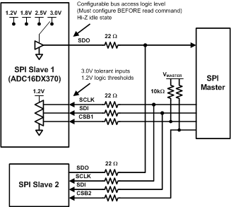 Figure 53. Typical SPI Application
9.2 Typical Application
The ADC16DX370 device is architected to fit seamlessly into most high intermediate frequency (IF) receiver applications where low noise and low distortion are required. An example block diagram is shown in Figure 54 where the ADC16DX370 device is used in the receive path as well as the transmitter observation path to accommodate digital pre-distortion. The 370-MHz sampling rate provides enough spectrum bandwidth and performance to support the newest cellular standards like LTE as well as the mature multi-carrier standards like GSM and UMTS with 100 MHz of bandwidth. The device supports diversity and MIMO architectures and multi-band receivers. The back-end JESD204B interface reduces the space required to transfer data and provides a standard interface that can migrate to future generations of products, making it optimal for highly-channelized applications.
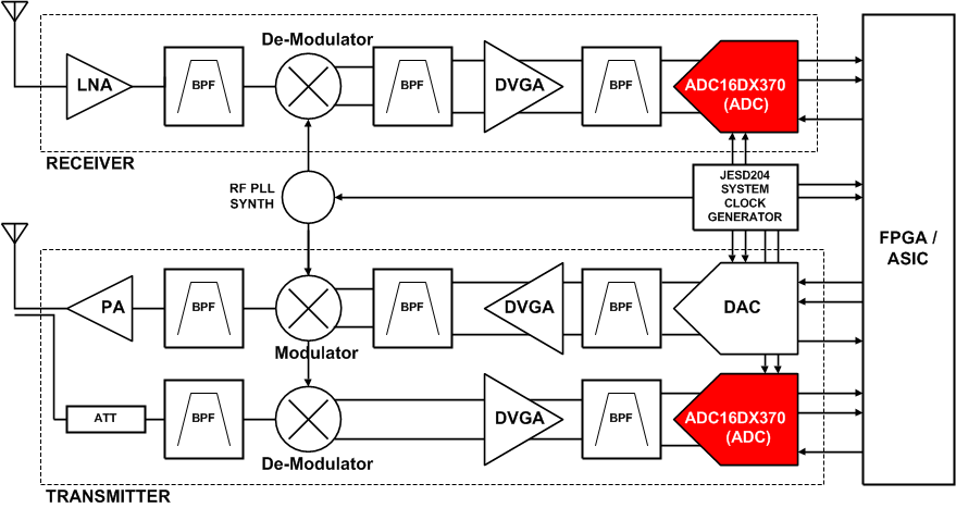 Figure 54. High IF Receiver and Transmitter With Digital Pre-Distortion Path
9.2.1 High-IF Sampling Receiver
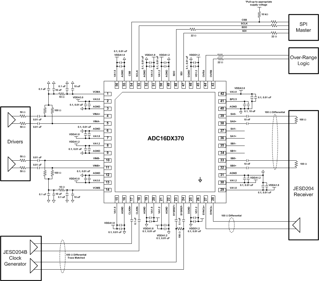 Figure 55. Typical Circuit Implementation
9.2.1.1 Design Requirements
The following are example design requirements expected of the ADC in a typical high-IF, 100-MHz bandwidth receiver, and is met by the ADC16DX370 device:
Table 32. Example Design Requirements for a High-IF Application
| Specification | Example Design Requirement(1) | ADC16DX370 Capability |
|---|---|---|
| Sampling rate | > 350-MSPS to allow 100-MHz unaliased bandwidth | Up to 370-MSPS |
| Input bandwidth | > 400-MHz, 1-dB flatness | 500-MHz, 1dB Bandwidth |
| Full-scale range | < 2-Vpp-diff | 1.7-Vpp-diff |
| Small signal noise spectral density | < –152-dBFS/Hz in a 100-MHz bandwidth | –152.7-dBFS/Hz in a 100-MHz bandwidth |
| Large-signal SNR | > 69-dBFS for a –3 dBFS, 150-MHz Input | 69.6-dBFS for a –3 dBFS, 150-MHz Input |
| SFDR | > 85-dBFS for a –3 dBFS, 150-MHz input | 88-dBFS for a –3 dBFS, 150-MHz input |
| HD2, HD3 | < –85-dBFS for a –3 dBFS, 150-MHz input | –88-dBFS for a –3 dBFS, 150-MHz input |
| Next largest SPUR | < –88-dBFS for a –3 dBFS, 150-MHz input | –90-dBFS for a –3 dBFS, 150-MHz input |
| Over-range detection | Included | Fast over-range detection on dedicated pins |
| Digital interface | JESD204B interface, 1 lane/channel, < 10-Gb/s bit rate | JESD204B subclass 1 interface, 1 lane/channel, 7.4-Gb/s bit rate |
| Configuration interface | SPI configuration, 4-wire, 1.8-V logic, SCLK up to 20-MHz | SPI configuration, 4-Wire, 1.8-V Logic, SCLK > 20-MHz |
| Package size | < 10 × 10 × 1 mm | 8 × 8 × 0.8 mm |
9.2.1.2 Design Procedure
The following procedure can be followed to design the ADC16DX370 device into most applications:
- Choose an appropriate ADC driver and analog input interface.
- Optimize the signal chain gain leading up to the ADC to make use of the full ADC dynamic range.
- Identify whether DC or AC coupling is required.
- Determine the desired analog input interface, such as a bandpass filter or a transformer.
- Use the provided input network models to design and verify the interface.
- Refer to the interface recommendations in Analog Input Considerations.
- Determine the core sampling rate of the ADC.
- Must satisfy the bandwidth requirements of the application .
- Must also provide enough margin to prevent aliasing or to accommodate the transitions bands of an anti-aliasing filter.
- Ensure the application initialization sequence properly handles ADC core calibration as described in ADC Core Calibration.
- Determine the system latency requirements.
- Total allowable latency through the ADC and JESD204B link.
- Is the system tolerant of latency variation over time or conditions or between power cycles?
- Determine the desired JESD204B link configuration as discussed in JESD204B Supported Features.
- Based on the system latency requirements, determine whether deterministic latency is required across the JESD204B link.
- Choose the number of lanes per channel, L, and verify that the device receiving the output serial data can accommodate the bit rate.
- Choose the number of frames per multi-frame, K.
- Choose whether scrambling is desired.
- Choose an appropriate clock generator, CLKIN interface, and SYSREF interface.
- Determine the system clock distribution scheme and the clock frequencies for the CLKIN and SYSREF inputs.
- Determine the allowable amount of sampling clock phase noise in the system and then select a CLKIN edge rate that satisfies this requirement as discussed in Clock Noise and Edge Rate.
- Choose an appropriate CLKIN interface as discussed in Driving the CLKIN+ and CLKIN– Input.
- Based on the latency requirements, determine whether SYSREF must meet setup and hold requirements relative to CLKIN.
- Choose the SYSREF signal type as discussed in SYSREF Signaling.
- Choose an appropriate SYSREF interface as discussed in Driving the SYSREF Input.
- Choose a CLKIN and SYSREF clock generator based on the above requirements. The signals need come from the same generator in some cases.
- Determine what clock idle modes are supported by the SYSREF clock generator and choose the appropriate setting for the SYSREF Offset feature as discussed in Effectively Using the SYSREF Offset and Detection Gate Features.
- Design the SYNCb interface as discussed in Driving the SYNCb Input.
- Choose appropriate configurations for the output serial data interface.
- Design the serial lane interface according to Output Serial-Lane Interface.
- Choose the required PCB materials, keeping in mind the desired rate of the serial lanes.
- Characterize the signal lane channels the connect the ADC serial output transmitters to the receiving device either through simulation or bench characterization.
- Optimize the VOD and DEM parameters to achieve the required signal integrity according to Voltage Swing and De-Emphasis Optimization.
- Design the SPI bus interface.
- Verify the electrical and functional compatibility of the ADC SPI with the SPI controller.
- Interface the ADC to the SPI bus according to SPI.
- Ensure that the application initialization sequence properly configures the output SDO voltage before the first read command.
- Design the power supply architecture and de-coupling.
- Choose appropriate power supply and supply filtering devices to provide stable, low-noise supplies as described in Power Supply Design.
- Design the capacitive de-coupling around the ADC, also described in Power Supply Design, while paying close attention to placing the capacitors as close to the device as possible.
- Time the power architecture to satisfy the power sequence requirements described in Power Supply Design.
- Ensure that the application initialization sequence satisfies the JESD204B link initialization requirements described in JESD204B Link Initialization.
9.2.1.3 Application Curve
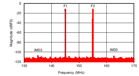
F1 = 145 MHz; F2 = 155 MHz