SBAS660C August   2016  – June 2017 ADS124S06 , ADS124S08

PRODUCTION DATA.  

  1. Features
  2. Applications
  3. Description
    1.     Device Images
      1.      Functional Block Diagram
  4. Revision History
  5. Device Family Comparison Table
  6. Pin Configuration and Functions
    1.     Pin Functions
  7. Specifications
    1. 7.1 Absolute Maximum Ratings
    2. 7.2 ESD Ratings
    3. 7.3 Recommended Operating Conditions
    4. 7.4 Thermal Information
    5. 7.5 Electrical Characteristics
    6. 7.6 Timing Characteristics
    7. 7.7 Switching Characteristics
    8. 7.8 Typical Characteristics
  8. Parameter Measurement Information
    1. 8.1 Noise Performance
  9. Detailed Description
    1. 9.1 Overview
    2. 9.2 Functional Block Diagram
    3. 9.3 Feature Description
      1. 9.3.1  Multiplexer
      2. 9.3.2  Low-Noise Programmable Gain Amplifier
        1. 9.3.2.1 PGA Input-Voltage Requirements
        2. 9.3.2.2 PGA Rail Flags
        3. 9.3.2.3 Bypassing the PGA
      3. 9.3.3  Voltage Reference
        1. 9.3.3.1 Internal Reference
        2. 9.3.3.2 External Reference
        3. 9.3.3.3 Reference Buffers
      4. 9.3.4  Clock Source
      5. 9.3.5  Delta-Sigma Modulator
      6. 9.3.6  Digital Filter
        1. 9.3.6.1 Low-Latency Filter
          1. 9.3.6.1.1 Low-Latency Filter Frequency Response
          2. 9.3.6.1.2 Data Conversion Time for the Low-Latency Filter
        2. 9.3.6.2 Sinc3 Filter
          1. 9.3.6.2.1 Sinc3 Filter Frequency Response
          2. 9.3.6.2.2 Data Conversion Time for the Sinc3 Filter
        3. 9.3.6.3 Note on Conversion Time
        4. 9.3.6.4 50-Hz and 60-Hz Line Cycle Rejection
        5. 9.3.6.5 Global Chop Mode
      7. 9.3.7  Excitation Current Sources (IDACs)
      8. 9.3.8  Bias Voltage Generation
      9. 9.3.9  System Monitor
        1. 9.3.9.1 Internal Temperature Sensor
        2. 9.3.9.2 Power Supply Monitors
        3. 9.3.9.3 Burn-Out Current Sources
      10. 9.3.10 Status Register
        1. 9.3.10.1 POR Flag
        2. 9.3.10.2 RDY Flag
        3. 9.3.10.3 PGA Output Voltage Rail Monitors
        4. 9.3.10.4 Reference Monitor
      11. 9.3.11 General-Purpose Inputs and Outputs (GPIOs)
      12. 9.3.12 Low-Side Power Switch
      13. 9.3.13 Cyclic Redundancy Check (CRC)
      14. 9.3.14 Calibration
        1. 9.3.14.1 Offset Calibration
        2. 9.3.14.2 Gain Calibration
    4. 9.4 Device Functional Modes
      1. 9.4.1 Reset
        1. 9.4.1.1 Power-On Reset
        2. 9.4.1.2 RESET Pin
        3. 9.4.1.3 Reset by Command
      2. 9.4.2 Power-Down Mode
      3. 9.4.3 Standby Mode
      4. 9.4.4 Conversion Modes
        1. 9.4.4.1 Continuous Conversion Mode
        2. 9.4.4.2 Single-Shot Conversion Mode
        3. 9.4.4.3 Programmable Conversion Delay
    5. 9.5 Programming
      1. 9.5.1 Serial Interface
        1. 9.5.1.1 Chip Select (CS)
        2. 9.5.1.2 Serial Clock (SCLK)
        3. 9.5.1.3 Serial Data Input (DIN)
        4. 9.5.1.4 Serial Data Output and Data Ready (DOUT/DRDY)
        5. 9.5.1.5 Data Ready (DRDY)
        6. 9.5.1.6 Timeout
      2. 9.5.2 Data Format
      3. 9.5.3 Commands
        1. 9.5.3.1  NOP
        2. 9.5.3.2  WAKEUP
        3. 9.5.3.3  POWERDOWN
        4. 9.5.3.4  RESET
        5. 9.5.3.5  START
        6. 9.5.3.6  STOP
        7. 9.5.3.7  SYOCAL
        8. 9.5.3.8  SYGCAL
        9. 9.5.3.9  SFOCAL
        10. 9.5.3.10 RDATA
        11. 9.5.3.11 RREG
        12. 9.5.3.12 WREG
      4. 9.5.4 Reading Data
        1. 9.5.4.1 Read Data Direct
        2. 9.5.4.2 Read Data by RDATA Command
        3. 9.5.4.3 Sending Commands When Reading Data
      5. 9.5.5 Interfacing with Multiple Devices
    6. 9.6 Register Map
      1. 9.6.1 Configuration Registers
        1. 9.6.1.1  Device ID Register (address = 00h) [reset = xxh]
          1. Table 26. Device ID (ID) Register Field Descriptions
        2. 9.6.1.2  Device Status Register (address = 01h) [reset = 80h]
          1. Table 27. Device Status (STATUS) Register Field Descriptions
        3. 9.6.1.3  Input Multiplexer Register (address = 02h) [reset = 01h]
          1. Table 28. Input Multiplexer (INPMUX) Register Field Descriptions
        4. 9.6.1.4  Gain Setting Register (address = 03h) [reset = 00h]
          1. Table 29. Gain Setting (PGA) Register Field Descriptions
        5. 9.6.1.5  Data Rate Register (address = 04h) [reset = 14h]
          1. Table 30. Data Rate (DATARATE) Register Field Descriptions
        6. 9.6.1.6  Reference Control Register (address = 05h) [reset = 10h]
          1. Table 31. Reference Control (REF) Register Field Descriptions
        7. 9.6.1.7  Excitation Current Register 1 (address = 06h) [reset = 00h]
          1. Table 32. Excitation Current Register 1 (IDACMAG) Register Field Descriptions
        8. 9.6.1.8  Excitation Current Register 2 (address = 07h) [reset = FFh]
          1. Table 33. Excitation Current Register 2 (IDACMUX) Register Field Descriptions
        9. 9.6.1.9  Sensor Biasing Register (address = 08h) [reset = 00h]
          1. Table 34. Sensor Biasing (VBIAS) Register Field Descriptions
        10. 9.6.1.10 System Control Register (address = 09h) [reset = 10h]
          1. Table 35. System Control (SYS) Register Field Descriptions
        11. 9.6.1.11 Offset Calibration Register 1 (address = 0Ah) [reset = 00h]
          1. Table 36. Offset Calibration Register 1 (OFCAL0) Register Field Descriptions
        12. 9.6.1.12 Offset Calibration Register 2 (address = 0Bh) [reset = 00h]
          1. Table 37. Offset Calibration Register 2 (OFCAL1) Register Field Descriptions
        13. 9.6.1.13 Offset Calibration Register 3 (address = 0Ch) [reset = 00h]
          1. Table 38. Offset Calibration Register 3 (OFCAL2) Register Field Descriptions
        14. 9.6.1.14 Gain Calibration Register 1 (address = 0Dh) [reset = 00h]
          1. Table 39. Gain Calibration Register 1 (FSCAL0) Register Field Descriptions
        15. 9.6.1.15 Gain Calibration Register 2 (address = 0Eh) [reset = 00h]
          1. Table 40. Gain Calibration Register 2 (FSCAL1) Field Descriptions
        16. 9.6.1.16 Gain Calibration Register 3 (address = 0Fh) [reset = 40h]
          1. Table 41. Gain Calibration Register 3 (FSCAL2) Field Descriptions
        17. 9.6.1.17 GPIO Data Register (address = 10h) [reset = 00h]
          1. Table 42. GPIO Data (GPIODAT) Register Field Descriptions
        18. 9.6.1.18 GPIO Configuration Register (address = 11h) [reset = 00h]
          1. Table 43. GPIO Configuration (GPIOCON) Register Field Descriptions
  10. 10Application and Implementation
    1. 10.1 Application Information
      1. 10.1.1 Serial Interface Connections
      2. 10.1.2 Analog Input Filtering
      3. 10.1.3 External Reference and Ratiometric Measurements
      4. 10.1.4 Establishing a Proper Input Voltage
      5. 10.1.5 Unused Inputs and Outputs
      6. 10.1.6 Pseudo Code Example
    2. 10.2 Typical Application
      1. 10.2.1 Design Requirements
      2. 10.2.2 Detailed Design Procedure
        1. 10.2.2.1 Register Settings
      3. 10.2.3 Application Curves
    3. 10.3 Do's and Don'ts
  11. 11Power Supply Recommendations
    1. 11.1 Power Supplies
    2. 11.2 Power-Supply Sequencing
    3. 11.3 Power-On Reset
    4. 11.4 Power-Supply Decoupling
  12. 12Layout
    1. 12.1 Layout Guidelines
    2. 12.2 Layout Example
  13. 13Device and Documentation Support
    1. 13.1 Device Support
      1. 13.1.1 Development Support
    2. 13.2 Documentation Support
      1. 13.2.1 Related Documentation
    3. 13.3 Related Links
    4. 13.4 Receiving Notification of Documentation Updates
    5. 13.5 Community Resources
    6. 13.6 Trademarks
    7. 13.7 Electrostatic Discharge Caution
    8. 13.8 Glossary
  14. 14Mechanical, Packaging, and Orderable Information

Package Options

Refer to the PDF data sheet for device specific package drawings

Mechanical Data (Package|Pins)
  • RHB|32
  • PBS|32
Thermal pad, mechanical data (Package|Pins)
Orderable Information

PGA Input-Voltage Requirements

As with many amplifiers, the PGA has an absolute input voltage range requirement that cannot be exceeded. The maximum and minimum absolute input voltages are limited by the voltage swing capability of the PGA output. The specified minimum and maximum absolute input voltages (VAINP and VAINN) depend on the PGA gain, the maximum differential input voltage (VINMAX), and the tolerance of the analog power-supply voltages (AVDD and AVSS). Use the maximum voltage expected in the application for VINMAX. The absolute positive and negative input voltages must be within the specified range, as shown in Equation 5:

Equation 5. AVSS + 0.15 V + |VINMAX| · (Gain – 1) / 2 < VAINP, VAINN < AVDD – 0.15 V – |VINMAX| · (Gain – 1) / 2

where

  • VAINP, VAINN = absolute input voltage
  • VINMAX = VAINP – VAINN = maximum differential input voltage

As mentioned in the previous section, PGA gain settings of 64 and 128 are scaled in the digital domain and are not implemented with the amplifier. When using the PGA in gains of 64 and 128, set the gain in Equation 5 to 32 to calculate the absolute input voltage range.

The relationship between the PGA input to the PGA output is shown graphically in Figure 51. The PGA output voltages (VOUTP, VOUTN) depend on the PGA gain and the input voltage magnitudes. For linear operation, the PGA output voltages must not exceed AVDD – 0.15 V or AVSS + 0.15 V. Note that the diagram depicts a positive differential input voltage that results in a positive differential output voltage.
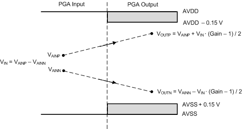
ADS124S06 ADS124S08 ai_pga_io_sbas660.gifFigure 51. PGA Input/Output Range

Download the ADS1x4S0x design calculator from www.ti.com. This calculator can be used to determine the input voltage range of the PGA.