SBAS660C August 2016 – June 2017 ADS124S06 , ADS124S08
PRODUCTION DATA.
- 1 Features
- 2 Applications
- 3 Description
- 4 Revision History
- 5 Device Family Comparison Table
- 6 Pin Configuration and Functions
- 7 Specifications
- 8 Parameter Measurement Information
-
9 Detailed Description
- 9.1 Overview
- 9.2 Functional Block Diagram
- 9.3
Feature Description
- 9.3.1 Multiplexer
- 9.3.2 Low-Noise Programmable Gain Amplifier
- 9.3.3 Voltage Reference
- 9.3.4 Clock Source
- 9.3.5 Delta-Sigma Modulator
- 9.3.6 Digital Filter
- 9.3.7 Excitation Current Sources (IDACs)
- 9.3.8 Bias Voltage Generation
- 9.3.9 System Monitor
- 9.3.10 Status Register
- 9.3.11 General-Purpose Inputs and Outputs (GPIOs)
- 9.3.12 Low-Side Power Switch
- 9.3.13 Cyclic Redundancy Check (CRC)
- 9.3.14 Calibration
- 9.4 Device Functional Modes
- 9.5 Programming
- 9.6
Register Map
- 9.6.1
Configuration Registers
- 9.6.1.1 Device ID Register (address = 00h) [reset = xxh]
- 9.6.1.2 Device Status Register (address = 01h) [reset = 80h]
- 9.6.1.3 Input Multiplexer Register (address = 02h) [reset = 01h]
- 9.6.1.4 Gain Setting Register (address = 03h) [reset = 00h]
- 9.6.1.5 Data Rate Register (address = 04h) [reset = 14h]
- 9.6.1.6 Reference Control Register (address = 05h) [reset = 10h]
- 9.6.1.7 Excitation Current Register 1 (address = 06h) [reset = 00h]
- 9.6.1.8 Excitation Current Register 2 (address = 07h) [reset = FFh]
- 9.6.1.9 Sensor Biasing Register (address = 08h) [reset = 00h]
- 9.6.1.10 System Control Register (address = 09h) [reset = 10h]
- 9.6.1.11 Offset Calibration Register 1 (address = 0Ah) [reset = 00h]
- 9.6.1.12 Offset Calibration Register 2 (address = 0Bh) [reset = 00h]
- 9.6.1.13 Offset Calibration Register 3 (address = 0Ch) [reset = 00h]
- 9.6.1.14 Gain Calibration Register 1 (address = 0Dh) [reset = 00h]
- 9.6.1.15 Gain Calibration Register 2 (address = 0Eh) [reset = 00h]
- 9.6.1.16 Gain Calibration Register 3 (address = 0Fh) [reset = 40h]
- 9.6.1.17 GPIO Data Register (address = 10h) [reset = 00h]
- 9.6.1.18 GPIO Configuration Register (address = 11h) [reset = 00h]
- 9.6.1
Configuration Registers
- 10Application and Implementation
- 11Power Supply Recommendations
- 12Layout
- 13Device and Documentation Support
- 14Mechanical, Packaging, and Orderable Information
Package Options
Refer to the PDF data sheet for device specific package drawings
Mechanical Data (Package|Pins)
- RHB|32
- PBS|32
Thermal pad, mechanical data (Package|Pins)
Orderable Information
7.1 Absolute Maximum Ratings(1)
| MIN | MAX | UNIT | ||
|---|---|---|---|---|
| Power-supply voltage | AVDD to AVSS | –0.3 | 5.5 | V |
| AVSS to DGND | –2.8 | 0.3 | ||
| DVDD to DGND | –0.3 | 3.9 | ||
| IOVDD to DGND | –0.3 | 5.5 | ||
| Analog input voltage | AINx, GPIOx, REFPx, REFNx, REFCOM | AVSS – 0.3 | AVDD + 0.3 | V |
| Digital input voltage | CS, SCLK, DIN, DOUT/DRDY, DRDY, START, RESET, CLK |
DGND – 0.3 | IOVDD + 0.3 | V |
| Input current | Continuous, AVSS-SW, REFN0, REFOUT | –100 | 100 | mA |
| Continuous, all other pins except power-supply pins | –10 | 10 | ||
| Temperature | Junction, TJ | 150 | °C | |
| Storage, Tstg | –60 | 150 | ||
(1) Stresses beyond those listed under Absolute Maximum Ratings may cause permanent damage to the device. These are stress ratings only, which do not imply functional operation of the device at these or any other conditions beyond those indicated under Recommended Operating Conditions. Exposure to absolute-maximum-rated conditions for extended periods may affect device reliability.

NOTE:
Single-byte communication is shown. Actual communication can be multiple bytes.
NOTE:
Single-byte communication is shown. Actual communication can be multiple bytes. Figure 3. RESET Pin and RESET Command Timing Requirements
 Figure 4. START/SYNC Pin Timing Requirements
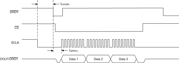
 Figure 6. Read Data Direct (Without an RDATA Command) Timing Requirements
 Figure 7. GPIO Switching Characteristics