SNAS602C FEBRUARY 2013 – December 2014 ADS1293
PRODUCTION DATA.
- 1 Features
- 2 Applications
- 3 Description
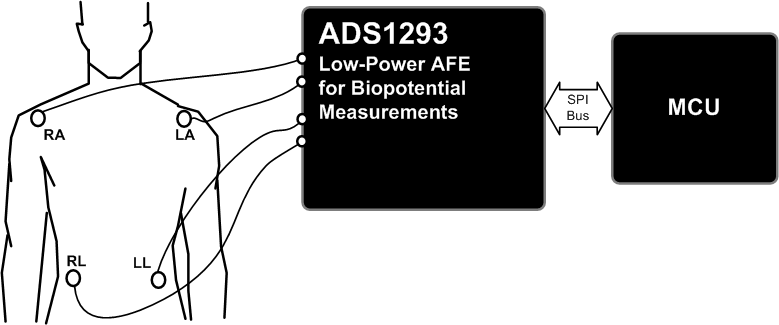
- 4 Application Diagram
- 5 Revision History
- 6 Pin Configuration and Functions
- 7 Specifications
-
8 Detailed Description
- 8.1 Overview
- 8.2 Functional Block Diagram
- 8.3
Feature Description
- 8.3.1 Flexible Routing Switch
- 8.3.2 Battery Monitoring
- 8.3.3 Test Mode
- 8.3.4 Analog Front-End
- 8.3.5 Instrumentation Amplifier (INA)
- 8.3.6 Sigma-Delta Modulator (SDM)
- 8.3.7 Programmable Digital Filters
- 8.3.8 Filter Settling Time
- 8.3.9 Analog Pace Channel
- 8.3.10 Wilson Reference
- 8.3.11 Common-Mode (CM) Detector
- 8.3.12 Right-Leg Drive (RLD)
- 8.3.13 Capacitive Load Driving
- 8.3.14 Error Status: RLD Rail
- 8.3.15 Lead-Off Detection (LOD)
- 8.3.16 DC Lead-Off Detect
- 8.3.17 Analog AC Lead-Off Detect
- 8.3.18 Digital AC Lead-Off Detect
- 8.3.19 Clock Oscillator
- 8.3.20 Synchronization
- 8.3.21 Single-Chip Multi-Channel Synchronization
- 8.3.22 Multichip Synchronization
- 8.3.23 Synchronization Errors
- 8.3.24 Alarm Functions
- 8.3.25 Error Filtering
- 8.3.26 ALARMB Pin and Error Masking
- 8.3.27 Error Register Automatic Clearing Description
- 8.3.28 Alarm Propagation
- 8.3.29 Reference Voltage Generators
- 8.3.30 Power Management
- 8.4 Device Functional Modes
- 8.5 Programming
- 8.6
Register Maps
- 8.6.1 Operation Mode Registers
- 8.6.2 Input Channel Selection Registers
- 8.6.3 Lead-Off Detect Control Registers
- 8.6.4 Common-Mode Detection and Right-Leg Drive Common-Mode Feedback Control Registers
- 8.6.5 Wilson Control Registers
- 8.6.6 Reference Registers
- 8.6.7 OSC Control Registers
- 8.6.8 AFE Control Registers
- 8.6.9 Error Status Registers
- 8.6.10 Digital Registers
- 8.6.11 Pace and ECG Data Read Back Registers
- 9 Application and Implementation
- 10Power Supply Recommendations
- 11Layout
- 12Device and Documentation Support
- 13Mechanical, Packaging, and Orderable Information
Package Options
Mechanical Data (Package|Pins)
- RSG|28
Thermal pad, mechanical data (Package|Pins)
Orderable Information
1 Features
- Three High-Resolution Digital ECG Channels With Simultaneous Pace Output
- EMI-Hardened Inputs
- Low Power: 0.3 mW/channel
- Input-Referred Noise: 7 µVpp (40-Hz Bandwidth)
- Input Bias Current: 175 pA
- Data Rate: Up to 25.6 ksps
- Differential Input Voltage Range: ±400 mV
- Analog Supply Voltage: 2.7 V to 5.5 V
- Digital I/O Supply Voltage: 1.65 V to 3.6 V
- Right-Leg Drive Amplifier
- AC and DC Lead-Off Detection
- Wilson and Goldberger Terminals
- ALARMB Pin for Interrupt Driven Diagnostics
- Battery Voltage Monitoring
- Built-In Oscillator and Reference
- Flexible Power-Down and Standby Modes
2 Applications
- Portable 1/2/3/5/6/7/8/12-Lead ECG
- Patient Vital Sign Monitoring: Holter, Event, Stress, and Telemedicine
- Automated External Defibrillator
- Sports and Fitness (Heart Rate and ECG)
3 Description
The ADS1293 incorporates all features commonly required in portable, low-power medical, sports, and fitness electrocardiogram (ECG) applications. With high levels of integration and exceptional performance, the ADS1293 enables the creation of scalable medical instrumentation systems at significantly reduced size, power, and overall cost.
The ADS1293 features three high-resolution channels capable of operating up to 25.6 ksps. Each channel can be independently programmed for a specific sample rate and bandwidth allowing users to optimize the configuration for performance and power. All input pins incorporate an EMI filter and can be routed to any channel through a flexible routing switch. Flexible routing also allows independent lead-off detection, right-leg drive, and Wilson/Goldberger reference terminal generation without the need to reconnect leads externally. A fourth channel allows external analog pace detection for applications that do not use digital pace detection.
The ADS1293 incorporates a self-diagnostics alarm system to detect when the system is out of the operating conditions range. Such events are reported to error flags. The overall status of the error flags is available as a signal on a dedicated ALARMB pin.
The device is packaged in a 5-mm × 5-mm × 0.8-mm, 28-pin LLP. Operating temperature ranges from –20°C to 85°C.
Device Information(1)
| PART NUMBER | PACKAGE | BODY SIZE (NOM) |
|---|---|---|
| ADS1293 | WQFN (28) | 5.00 mm x 5.00 mm |
- For all available packages, see the orderable addendum at the end of the datasheet.
4 Application Diagram