SNAS602C FEBRUARY 2013 – December 2014 ADS1293
PRODUCTION DATA.
- 1 Features
- 2 Applications
- 3 Description
- 4 Application Diagram
- 5 Revision History
- 6 Pin Configuration and Functions
- 7 Specifications
-
8 Detailed Description
- 8.1 Overview
- 8.2 Functional Block Diagram
- 8.3
Feature Description
- 8.3.1 Flexible Routing Switch
- 8.3.2 Battery Monitoring
- 8.3.3 Test Mode
- 8.3.4 Analog Front-End
- 8.3.5 Instrumentation Amplifier (INA)
- 8.3.6 Sigma-Delta Modulator (SDM)
- 8.3.7 Programmable Digital Filters
- 8.3.8 Filter Settling Time
- 8.3.9 Analog Pace Channel
- 8.3.10 Wilson Reference
- 8.3.11 Common-Mode (CM) Detector
- 8.3.12 Right-Leg Drive (RLD)
- 8.3.13 Capacitive Load Driving
- 8.3.14 Error Status: RLD Rail
- 8.3.15 Lead-Off Detection (LOD)
- 8.3.16 DC Lead-Off Detect
- 8.3.17 Analog AC Lead-Off Detect
- 8.3.18 Digital AC Lead-Off Detect
- 8.3.19 Clock Oscillator
- 8.3.20 Synchronization
- 8.3.21 Single-Chip Multi-Channel Synchronization
- 8.3.22 Multichip Synchronization
- 8.3.23 Synchronization Errors
- 8.3.24 Alarm Functions
- 8.3.25 Error Filtering
- 8.3.26 ALARMB Pin and Error Masking
- 8.3.27 Error Register Automatic Clearing Description
- 8.3.28 Alarm Propagation
- 8.3.29 Reference Voltage Generators
- 8.3.30 Power Management
- 8.4 Device Functional Modes
- 8.5 Programming
- 8.6
Register Maps
- 8.6.1 Operation Mode Registers
- 8.6.2 Input Channel Selection Registers
- 8.6.3 Lead-Off Detect Control Registers
- 8.6.4 Common-Mode Detection and Right-Leg Drive Common-Mode Feedback Control Registers
- 8.6.5 Wilson Control Registers
- 8.6.6 Reference Registers
- 8.6.7 OSC Control Registers
- 8.6.8 AFE Control Registers
- 8.6.9 Error Status Registers
- 8.6.10 Digital Registers
- 8.6.11 Pace and ECG Data Read Back Registers
- 9 Application and Implementation
- 10Power Supply Recommendations
- 11Layout
- 12Device and Documentation Support
- 13Mechanical, Packaging, and Orderable Information
Package Options
Mechanical Data (Package|Pins)
- RSG|28
Thermal pad, mechanical data (Package|Pins)
Orderable Information
8 Detailed Description
8.1 Overview
The ADS1293 is a fully-integrated signal chain for ECG applications. It features three low-power, 24-bit resolution channels for ECG and pace monitoring and an auxiliary fourth channel for analog pace detection. In addition, the ADS1293 features AC and DC lead-off detection, right-leg drive capability, and Wilson and Goldberger terminals.
Each of the three channels is synchronized and provides digital filtering with a cut-off frequency that is programmable from 5 Hz to 1280 Hz. Each channel filter can be set independently while maintaining synchronization. In addition, a lower-resolution output is provided for each signal channel with a cut-off frequency programmable between 650 Hz to 2.6 kHz. These output signals are ideal for sensing a pace-maker signal. Each channel provides enough dynamic range to handle electrode offset and motion artifacts without sacrificing resolution. Each input has built-in EMI rejection that eliminates noise from RF transmitters.
8.2 Functional Block Diagram
8.3 Feature Description
8.3.1 Flexible Routing Switch
The flexible routing switch can connect the inputs of the three analog front-end channels as well as the inputs of the analog pace channel to any of the 6 input pins. This allows system flexibility and even on-the-fly reconfiguration of the ECG monitoring system. For test purposes, the flexible routing switch can short the differential input pins of a channel or connect a differential reference signal to the input of a channel. This reference voltage can be applied with both positive and negative polarity. This feature allows to measure relative mismatches between channels, such as offset and gain mismatches. Additionally, there is an option to route a fraction of the battery voltage (the voltage source connected to the VDD pin) to an input channel. This allows the ADS1293 to monitor the state of charge of the battery.
The switch path inside the flexible routing switch is illustrated in Figure 17. The figure shows the switch path for a single channel. All channels are completely identical. The switches are controlled by the registers FLEX_CH1_CN, FLEX_CH2_CN, FLEX_CH3_CN, and FLEX_VBAT_CN, which are described in the Input Channel Selection Registers.
 Figure 17. Flexible Routing Switch for Channel 1
It should be noted that the switches that control the input selection for the analog front-end channels have a certain priority. If the battery voltage monitoring mode is enabled by programming the VBAT_MONI_CHx bit in the FLEX_VBAT_CN register, then the POSx and NEGx bits programmed in the FLEX_CHx_CN register no longer have any effect. The battery voltage monitoring mode thus takes priority; this is shown in the first row of Table 1. Furthermore, the test features take second priority over the input pin selection. If the TSTx bit of the FLEX_CHx_CN register are not zero, then the POSx and NEGx bits are essentially ignored, and the test features will take priority as seen in Table 1. The TSTx, POSx, and NEGx bits are described in the Input Channel Selection Registers.
Table 1. Channel 1 Switch Configuration
| VBAT_MONI_CHx | CALx | POSx | NEGx | MODE |
|---|---|---|---|---|
| 1 | X | X | X | CHx is in battery voltage monitoring mode |
| 0 | 11 | X | X | CHx input shorted |
| 0 | 01 | X | X | CHx input connected to positive reference |
| 0 | 10 | X | X | CHx input connected to negative reference |
| 0 | 00 | INx | INy | CHx positive input connected to pin INx and negative input connected to pin INy |
8.3.2 Battery Monitoring
The battery voltage monitoring mode is enabled by setting bit VBAT_MONI_CHx = 1 in the FLEX_VBAT_CN register. Also, the instrumentation amplifier of the selected channel must be shut down by setting SHDN_INA_CHx = 1 in the AFE_SHDN_CN register. In this mode, the positive input, POSx, of the sigma-delta modulator will sample the voltage supplied on the VDD pin. At the same time, the negative input, NEGx, of the sigma-delta modulator will sample the reference voltage, VREF, generated on or provided to the CVREF pin. As a result, the output signal of the sigma-delta modulator is a measure for (VBAT-VREF). In this operation, the sigma-delta modulator works with a modified gain factor, and the battery voltage, VBAT, can be calculated as follows:
In this equation, VREF equals 2.4 V if the internal reference voltage generator is used, and ADCMAX represents the maximum output code of the ADC, which would correspond to a theoretical 2.4-V signal at the input of the sigma-delta modulator. The value of ADCMAX is dependent on the configuration of the digital filters, and the corresponding ADCMAX values are listed in Table 8 through Table 11.
The battery monitoring mode is targeted for battery operated systems within a voltage range of 2.4 V to 4.8 V. The battery monitoring mode cannot be used when the ADS1293 is powered from a regulated 5-V supply because it risks saturating the sigma-delta modulator. There is a also a low battery alarm that is implemented independently from the battery monitoring mode, which will trigger a battery alarm when the supply voltage is below 2.7 V (see the BATLOW description in Alarm Functions).
8.3.3 Test Mode
If the battery voltage monitoring function is not enabled, and if bit TSTx = 01 (see the Input Channel Selection Registers section), then a positive DC test signal is provided to the input of the instrumentation amplifier. If TSTx = 10, then that same test signal is provided but with negative polarity. The expected ADC output code can be calculated as follows:

In Equation 2, the positive or negative DC test signal VTEST = VREF/12. Note that this test mode is not a gain calibration since VTEST and VREF are generated by the same reference; however, it can be used as a self-test or to measure gain mismatches between channels.
When TSTx = 11, the inputs of the instrumentation amplifier in the channel can be shorted to provide a zero test signal. The expected ADC output code equation can be simplified to:
For both equations, the value of ADCMAX corresponding to a given decimation configuration can be obtained from Table 8 through Table 11.
8.3.4 Analog Front-End
The ADS1293 contains three analog front ends that convert a differential analog voltage into a digital signal. Each analog front end consists of an instrumentation amplifier (INA), a sigma-delta modulator (SDM), and a digital filter.
8.3.5 Instrumentation Amplifier (INA)
The instrumentation amplifier provides a high input impedance to interface with signal sources that may have relatively high output impedance, such as ECG electrodes. The maximum differential input voltage range of the Sigma-Delta Modulator (SDM) behind the INA is ±1.4 V, and the gain of the INA is 3.5x. Therefore, the maximum differential input voltage of the INA is ±400 mV.
The input common-mode voltage range (CMVR) of the INA is 0.95 V to VDD-0.95 V. If the input differential voltage range is limited to smaller values, then the CMVR can be somewhat extended. If the differential input signal is limited to VINMAX, the CMVR range can be defined as:

The INA can be configured to operate in a low-power mode or in a high-resolution mode. The low-power mode consumes about 3 times less power than the high-resolution mode. However, the high-resolution mode has less noise than the low-power mode. Switching between these two modes is controlled by the EN_HIRES_CHx bits in the AFE_RES register.
When a channel is not in use, its INA can be shut down by programming the SHDN_INA_CHx bit in the AFE_SHDN_CN register, and its SDM can also be shut down by programming the SHDN_SDM_CHx bit in the AFE_SHDN_CN register.
8.3.5.1 Instrumentation Amplifier Fault Detection
The output signal of the instrumentation amplifier can be monitored to ensure its output signal is within an appropriate range. The out-of-range error flags for the INAs can be observed in the ERROR_RANGE1, ERROR_RANGE2 and ERROR_RANGE3 registers.
The output signal is present at two points: OUTP and OUTN. If the input common-mode voltage or differential voltage is such that the instrumentation amplifier would have to drive the voltages at these points above the positive or below the negative supply rail, then the signal accuracy would be lost. These two points are monitored and a warning flag is raised if the voltage on these pins approaches the supply rails. If the OUTP_HIGH flag is raised, then the voltage at OUTP is close to the positive rail. This indicates the differential input signal is too large or the input common-mode voltage is too high. If the OUTP_LOW flag is raised, then the voltage at OUTP is close to the negative rail. This happens at low input common-mode voltages and large negative differential input voltages. Similar reasoning holds for the OUTN_HIGH and OUTN_LOW flags.
The differential output voltage of the INA is monitored and reported to the DIF_HIGH bit. This error flag indicates that the differential signal is out-of-range and is no longer an accurate representation of the input signal. The DIF_HIGH error flag is raised if the differential output voltage of the INA exceeds ±1.4 V, which is the input range of the Delta-Sigma Modulator. When this happens, the SDM will no longer sample the output of the INA, but instead will sample 0 V. The sign of the input signal can still be observed in the SIGN bit of the ERROR_RANGEx registers.
The fault detection circuitry for OUTP_HIGH, OUTP_LOW, OUTN_HIGH and OUTN_LOW can be shut down by programming the SHDN_FAULTDET_CHx bits in the AFE_FAULT_CN register. These shutdown bits do not affect the operation of DIF_HIGH and SIGN because the instrumentation amplifier should always provide these signals to the sigma-delta modulator. The circuitry that generates DIF_HIGH and SIGN only gets shut down when the corresponding INA is shut down.
8.3.6 Sigma-Delta Modulator (SDM)
The Sigma-Delta Modulator (SDM) takes the output signal of the INA and converts this signal into a high resolution bit stream that is further processed by the digital filters.
The SDM can operate at clock frequencies of 102.4 kHz or 204.8 kHz; these frequencies are generated internally. Running the SDM at 204.8 kHz results in a larger oversampling ratio, which improves the resolution of the signal recovered by the digital filters behind the SDM. However, running the SDM at a higher clock frequency will increase its power consumption, resulting in a tradeoff between resolution and power consumption.
The 102.4-kHz or 204.8-kHz clock frequency can be selected for each channel individually by programming the FS_HIGH_CHx bits in the AFE_RES register.
The SDM also features dithering to reduce tones in the system, a known by-product of Sigma-Delta converters. The dithering circuit is active by default and is automatically turned OFF when the input signal is larger than 40 mV.
8.3.6.1 Sigma-Delta Modulator Fault Detection
The state of the integrators in the Sigma-Delta Modulator (SDM) are monitored to detect over-range signals that cause the SDM to become unstable. When an over-range event is detected in the SDM, the state of its integrators is reset, and the over-range error is reported to the SDM_OR_CHx bits of the ERROR_RANGE1, ERROR_RANGE2, and ERROR_RANGE3 registers.
8.3.7 Programmable Digital Filters
A programmable digital filter behind the Sigma-Delta Modulator (SDM) reconstructs the signal from the SDM output bit stream. The filter consist of three programmable SINC filters as shown in Figure 18. Each stage is a fifth order SINC filter.
 Figure 18. Sinc Filters
The decimation rates (R1, R2, and R3) of the SINC filters are programmable as described in Table 2. Each of the three stages further filters and decimates the bit stream so that the output data rate (ODR) and bandwidth (BW) of the signal is reduced, and at the same time, the resolution is enhanced. A 16-bit digital signal with relatively high ODR and BW, but with somewhat limited resolution, is available after the second stage; this signal can be used for PACE pulse detection. That signal is further decimated by the third stage and results in a very high-resolution filtered 24-bit digital signal that is an accurate representation of the ECG signal.
Table 2. Programmable Digital Filter Coefficients
| Stage 1 (R1) | Stage 2 (R2) | Stage 3 (R3) |
|---|---|---|
| 4 (Standard PACE Data Rate), 2 (Double PACE Data Rate) | 4, 5, 6, 8 | 4, 6, 8, 12, 16, 32, 64, 128 |
The first stage sets the Standard PACE Data Rate (where the decimation rate R1 = 4) or the Double PACE Data Rate (where R1 = 2). Operating the device in the Double PACE Data Rate will double the ODR for the first stage (and therefore also for the subsequent stages). However, the BW of the first stage does not change in this mode; only the ODR is affected. By operating the device in the Double PACE Data Rate, the ODR of the PACE data is doubled, and thus, more accurate PACE pulse detection is possible. However, operating the device in the Double PACE Data Rate will increase its power consumption. The R1 decimation rate can be programmed for each of the three channels separately by using the R1_RATE register.
Programming the second stage (R2) to a low decimation rate sets a relatively high ODR and BW, but doing so will also increase the noise level. For digital PACE pulse detection, smaller values for R2 are recommended. The R2 decimation rate can be programmed using the R2_RATE register.
As the third stage decimation (R3) increases, the ODR and BW of the ECG decreases. When detecting an ECG signal, higher values of R3 are recommended. The R3 decimation rate for each channel can be individually programmed using the R3_RATE_CH1, R3_RATE_CH2, and R3_RATE_CH3 registers.
Table 8, Table 9, Table 10, and Table 11 illustrate how these decimation rates R1, R2, and R3 affect the ODR, BW, and RMS Noise of the PACE and ECG signals. In addition, the ODR and BW also depend on whether the SDM is running at a low (102.4kHz) or high (204.8 kHz) clock frequency (set by the FS_HIGH_CHx bits in the AFE_RES register). The RMS Noise of the PACE and ECG channels also depend on whether the instrumentation amplifier is running in low-power or high-resolution mode (set by the EN_HIRES bits in the AFE_RES register).
In summary, the output data rate of an ECG channel can be calculated as follows:
And the output data rate of a PACE channel can be calculated as follows:
Where fS is the clock frequency of the modulator: 102.4 kHz, or 204.8 kHz.
8.3.8 Filter Settling Time
The low-pass filter frequency responses of the ECG and PACE SINC filters result in a settling time associated with their outputs as a response to a step input signal. This settling time is determined by the order of the filter, N, its differential delay, M, and the channel output data rate, ODR:
The ODR of the filter is a function of the sigma-delta's sampling frequency, fS, and the filter decimation rates. The value of the ODR can be calculated using Equation 5 and Equation 6. For an ECG channel, the value of NxM = 5. For a pace channel NxM = 5 when operated in the Standard Pace Data Rate (R1 = 4), and NxM = 10 when operated in the Double Pace Data Rate (R1 = 2).
As a result, an unclamped pace signal applied to the filter input results in an ECG channel minimum settling time of:
A Standard Pace Data Rate operated pace channel will go through a minimum settling time of:
And a Double Pace Data Rate operated pace channel will go through a minimum settling time of:
8.3.9 Analog Pace Channel
The ADS1293 features an additional analog pace channel to process pulses from a pacemaker. The analog pace channel is suitable for low-power applications where the device can be configured for low data rates in ECG mode only, while an analog channel detects PACE pulses. This channel consists of a traditional three opamp instrumentation amplifier and is designed to amplify an ECG signal in a typical bandwidth, as specified in the Electrical Characteristics table, allowing for external circuitry to detect the PACE pulses. The analog pace implementation inside the ADS1293 is depicted in Figure 19. The analog pace channel is not limited to PACE detection; it is a full-analog channel that could be used to pre-amplify signals, for instance, from a respiration sensor.
The output voltage of the analog pace channel is:
Where Vinp and Vinm are the positive and negative inputs of the analog pace channel. The input pins of this channel can be selected in the FLEX_PACE_CN register and can connect to any of the IN1 through IN6 pins. Note there is no battery monitoring option available through this channel. There is, however, the reference voltage test mode available as described in Test Mode.
 Figure 19. Analog Pace Channel Instrumentation Amplifier
The output of the analog pace channel can be multiplexed to the WCT or RLDIN pin using the AFE_PACE_CN register. When PACE2RLDIN = 1, the output is routed to the RLDIN terminal, while internally the positive input of the Right-Leg Drive amplifier is connected to the RLDREF pin. When PACE2WCT = 1, the output is routed to the WCT terminal, and the WCT terminal is disconnected from the Wilson output. In this case, the Wilson output can still be connected internally to the IN6 pin using the WILSON_CN register. The analog pace channel is disabled when SHDN_PACE = 1 to save power when it is not used.
The analog pace channel is designed to drive a high pass filter and can directly drive a capacitive load of 100 pF.
For analog pace detection, TI recommends having a band pass filter at the output of the analog pace channel, amplify the resulting signal with a relatively high bandwidth amplifier, and compare the amplified pulses with a relatively high speed window comparator. The bandwidth of the band pass filter, gain of the amplification, and the thresholds of the window comparator should be tuned so the comparators trigger on pacemaker pulses, but not to other signals present in the ECG environment.
8.3.10 Wilson Reference
The ADS1293 features a Wilson reference block consisting of three buffer amplifiers and resistors that can generate the voltages for the Wilson Central Terminal or Goldberger terminals. Each of the three buffer amplifiers can be connected to any input pin, IN1 through IN6, by programming the WILSON_EN1, WILSON_EN2, and WILSON_EN3 registers. A buffer that is not connected to an input pin is automatically disabled. When disabled, the buffers have a high-output impedance.
 Figure 20. Wilson Reference Generator Circuit
The output of the Wilson Reference can be routed internally to IN6, and the outputs of the Goldberger reference can be routed internally to IN4, IN5 and IN6. This is configured in the WILSON_CN register. If routed externally, TI strongly recommends shielding these connections, which due to their high-output impedance, are prone to pick up external interference.
8.3.10.1 Wilson Central Terminal
There are three main ECG leads that are measured differentially:
- Lead I: I = LA - RA
- Lead II: II = LL - RA
- Lead III: III = LL - LA
Where LA is the left-arm electrode, LL is the left-leg electrode, and RA is the right-arm electrode.
In a standard 5-lead or 12-lead ECG, the Wilson Central Terminal is used as the reference voltage for the chest electrodes, which are measured differentially against this reference. The Wilson Central Terminal is defined as the average of the three limb electrodes, RA, LA, and LL:
Wilson Central Terminal = (RA + LA + LL)/3
The output of Wilson Central Terminal generated by the ADS1293, as seen in Figure 20, is defined as:
WCTOUT = (BUF1 + BUF2 + BUF3)/3
The user could program the WILSON_EN1 register to connect the RA electrode to BUF1, program the WILSON_EN2 register to connect the LA electrode to BUF2, and program the WILSON_EN3 register to connect the LL electrode to BUF3.
When the Wilson reference is enabled, its output is present at the WCT pin, except when the analog pace channel is routed to the WCT pin (see Analog Pace Channel). In such a configuration, the Wilson terminal can still be made available at an external pin by programming the WILSONINT bit to 1. Setting this bit connects the output of the Wilson reference internally to the IN6 pin.
8.3.10.2 Goldberger Terminals
Augmented leads in 3-lead, 5-lead or 12-lead ECG are typically calculated digitally based on the measurement results of Lead I and Lead II. The augmented leads are defined as:
- aVR = -(I + II)/2 = RA - (LA + LL)/2 = RA - G1
- aVL = I - II/2 = LA - (RA + LL)/2 = LA - G2
- aVF = II - I/2 = LL - (RA + LA)/2 = LL - G3
Augmented leads can also be measured directly with the Goldberger terminals to give the best SNR. The Goldberger terminals generated by the ADS1293, as seen in Figure 20, are defined as:
- G1 = (BUF2 + BUF3)/2
- G2 = (BUF1 + BUF3)/2
- G3 = (BUF1 + BUF2)/2
In this case, the user must program the WILSON_EN1 register to connect the RA electrode to BUF1, program the WILSON_EN2 register to connect the LA electrode to BUF2, and program the WILSON_EN3 register to connect the LL electrode to BUF3.
The Goldberger output terminals, G1, G2 and G3 can be made available on external pins programming the GOLDINT bit to 1. Setting this bit connects the Goldberger terminals internally to the IN4, IN5 and IN6 pins.
- IN4 = G1
- IN5 = G2
- IN6 = G3
Note that multiple ADS1293 chips are required if both the augmented leads and the three basic leads need to be converted directly.
The WILSONINT and GOLDINT bits must not be programmed to 1 simultaneously because it will short-circuit the Wilson output terminal and the third Goldberger output terminal. The options described in these sections are summarized in Table 3.
Table 3. Wilson and Goldberger Reference Control
| GOLDINT | WILSONINT | PACE2WCT | TERMINAL OUTPUTS | |||
|---|---|---|---|---|---|---|
| WCT PIN | IN4 PIN | IN5 PIN | IN6 PIN | |||
| 0 | 0 | 0 | WCTOUT | General input | General input | General input |
| 0 | 1 | 0 | WCTOUT | General input | General input | WCTOUT |
| 1 | 0 | 0 | WCTOUT | (BUF2 + BUF3)/2 | (BUF1 + BUF3)/2 | (BUF1 + BUF2)/2 |
| 1 | 1 | X | Illegal | Illegal | Illegal | Illegal |
| 0 | 0 | 1 | Vpaceout | General input | General input | General input |
| 0 | 1 | 1 | Vpaceout | General input | General input | WCTOUT |
| 1 | 0 | 1 | Vpaceout | (BUF2 + BUF3)/2 | (BUF1 + BUF3)/2 | (BUF1 + BUF2)/2 |
8.3.11 Common-Mode (CM) Detector
The Common-Mode Detector averages the voltage of up to six input pins. Its output can be used in a right-leg drive feedback circuit. The selection of the input pins that contribute to the average is configured in the CMDET_EN register. The Common-Mode Detector is automatically disabled when no input pin is selected.
 Figure 21. Common-Mode Detector Circuit
8.3.11.1 Cable Shield Driving
The Common-Mode Detector also has a programmable capacitive load driving capability of up to 8 nF that allows it to drive a cable shield to reduce the common-mode signal current through a cable. This effectively increases the bandwidth of the filter formed by the electrode impedance and the cable capacitance, reducing the amount of common-mode to differential mode crosstalk. As a result, the CMRR of the overall ECG system is improved.
The bandwidth and capacitive load driving capability of the Common-Mode Detector can be configured in the CMDET_CN register to achieve an optimal tradeoff with power consumption. Table 4 lists the power consumption corresponding to different configuration scenarios given that all inputs are enabled by setting the CMDET_EN register = 0x3F.
The lowest current consumption setting can be used when the Common-Mode Detector is only used to drive the Right-Leg Driver, and no cable shield is driven. If a cable shield needs to be driven, the power can be increased to drive the cable capacitance depending on the number and type of the driven cable shields. Note that the capacitive driving capability is reduced in the higher bandwidth mode.
Table 4. Typical Common-Mode Detector Bandwidth, Capacitive Drive and Power Consumption
| CMDET_BW | CMDET_CAPDRIVE | BW (kHz) |
CLOAD
(nF) |
CMDET ISUPPLY
(µA) |
|---|---|---|---|---|
| 0: Low BW mode | 00: Low Cap Drive | 50 | 2 | 39 |
| 0: Low BW mode | 01: Medium Low Cap Drive | 50 | 3.3 | 45 |
| 0: Low BW mode | 10: Medium High Cap Drive | 50 | 4.5 | 56 |
| 0: Low BW mode | 11: High Cap Drive | 50 | 8 | 75 |
| 1: High BW mode | 00: Low Cap Drive | 150 | 0.4 | 43 |
| 1: High BW mode | 01: Medium Low Cap Drive | 150 | 0.65 | 49 |
| 1: High BW mode | 10: Medium High Cap Drive | 150 | 1 | 60 |
| 1: High BW mode | 11: High Cap Drive | 150 | 1.6 | 79 |
8.3.11.2 Common-Mode Output Range (CMOR)
The Common-Mode Detector incorporates an out-of-range alarm to sense if the common-mode voltage is outside of the common-mode voltage range of the ADS1293. A Common-Mode Out-of-Range Alarm is created in the CMOR bit of the ERROR_STATUS register when the common-mode drops below 0.75 V or exceeds VDD-0.75 V. System alarms are filtered by the digital circuitry (see Error Filtering), and for this reason, the master clock must be active in order to capture an alarm.
8.3.12 Right-Leg Drive (RLD)
The RLD is a programmable operational amplifier that is intended to control the common-mode level of the patient connected through electrodes to the ADS1293 and thereby improving the AC CMRR of the overall ECG system. In a typical ADS1293 application, the common-mode level of the patient's body is measured by the Common-Mode Detector described in the previous section. The CMOUT is compared by the RLD to the reference voltage present on the RLDREF pin. When used in an inverting amplifier topology, the right-leg electrode is driven by the RLD to counter any differences between the reference voltage and the detected common-mode level. This reduces the amount of power-line common-mode interference.
The negative input terminal of the RLD op-amp is always connected to the RLDINV pin. By default, the positive input terminal of the RLD op-amp is routed to the RLDIN pin. However, when bit PACE2RLDIN = 1 in the AFE_PACE_CN register, the positive input terminal is routed to the internally to the RLD reference. This will allow connecting the output of the analog pace instrumentation amplifier to the RLDIN pin. The output of the RLD operational amplifier is always connected to the RLDOUT pin, and in addition, can be connected to one of the IN1-IN6 terminals by programming the SELRLD bit in the RLD_CN register. The RLD circuit can be shut down in the same register by setting bit SHDN_RLD = 1.
 Figure 22. Right-Leg Drive Circuit
8.3.13 Capacitive Load Driving
The bandwidth and capacitive load driving capability of the RLD can be configured in the RLD_CN register to achieve an optimal tradeoff of power consumption. Table 5 lists the power consumption corresponding to different configuration scenarios.
Table 5. Typical Right-Leg Drive Bandwidth, Capacitive Drive, and Power Consumption
| RLD_BW | RLD_CAPDRIVE | GBW (kHz) |
CLOAD
(nF) |
RLD ISUPPLY
(µA) |
|---|---|---|---|---|
| 0: Low BW mode | 00: Low Cap Drive | 50 | 2 | 20 |
| 0: Low BW mode | 01: Medium Low Cap Drive | 50 | 3.3 | 25 |
| 0: Low BW mode | 10: Medium High Cap Drive | 50 | 4.5 | 36 |
| 0: Low BW mode | 11: High Cap Drive | 50 | 8 | 55 |
| 1: High BW mode | 00: Low Cap Drive | 200 | 0.4 | 23 |
| 1: High BW mode | 01: Medium Low Cap Drive | 200 | 0.65 | 29 |
| 1: High BW mode | 10: Medium High Cap Drive | 200 | 1 | 39 |
| 1: High BW mode | 11: High Cap Drive | 200 | 1.6 | 60 |
8.3.14 Error Status: RLD Rail
The RLD amplifier incorporates a near to rail alarm function that is triggered when the output of the op-amp is below 0.2 V or above VDD-0.2 V. The alarm is reported to the RLDRAIL bit in the ERROR_STATUS register and indicates that the RLD's feedback loop has difficulty maintaining a constant voltage on the patient’s body. In this case, the common-mode on the patient’s body may drift away from its target value, but it may still be within the proper input common-mode voltage range of the ADS1293, and the ECG signal data acquisition can continue. When the common-mode on the patient’s body is outside the operation range of the ADS1293, the CMOR error will be raised, as described in the previous section. System alarms are filtered by the digital circuitry (see Error Filtering), and for this reason, the master clock must be active in order to capture an alarm.
8.3.15 Lead-Off Detection (LOD)
The lead-off detect (LOD) block of the ADS1293 can be used to monitor the connectivity of the 6 input pins to electrodes. The LOD block injects a programmable DC or AC excitation current into selected input pins and detects the voltages that appear on the input pins in response to that current. If a lead is not making a proper contact, then the electrode impedance will be high, and as a result, the voltage in response to a small test current will be relatively large, while the voltage for a well-connected lead will be small.
The LOD block can work in one of the three following modes: 1) DC lead-off detect, 2) analog AC lead-off detect or 3) digital AC lead-off detect. All three LOD modes use a common DAC that provides a programmable reference current. This reference current is used to set the magnitude of the test current for lead-off detection. The amplitude of the excitation current used for lead-off detection can be programmed in the LOD_CURRENT register, where codes 0 to 255 result in currents ranging from 0 to 2.040 µA in steps of 8 nA.
The complete LOD block can be shut down by programming the SHDN_LOD bit to 1 in the LOD_CN register.
8.3.16 DC Lead-Off Detect
The LOD block can be configured for DC LOD mode by programming a 0 in the SELAC_LOD bit of the LOD_CN register. In the DC LOD mode, a DC test current can be injected into any of the six input pins by setting the corresponding bit EN_LOD[x] of the LOD_EN register. Programming a bit to 1 in this register enables a switch that allows a copy of the current programmed into the DAC to be injected into the desired input pins, as shown in the simplified block diagram of Figure 23.
 Figure 23. Simplified DC Lead-Off Detect Block Diagram
For the selected input pins, a Schmitt-trigger comparator then compares the voltage that appears on the pin to (VDD-0.5 V). The result of this comparison can be accessed through the corresponding OUT_LOD[x] bit of the ERROR_LOD register. If a lead is off, then the injected current has no return path-to-ground, and as a result, the voltage on the associated input pin will rise towards VDD. This is detected by the comparator and is used as a signal to indicates the lead is not properly connected.
It is important to note that the lead-off detection circuit requires a low impedance return path from the right-leg electrode-to-ground, such as a voltage reference or the RLD amplifier output. Without a proper low impedance return path for the LOD currents, all enabled LOD pins will report a lead disconnected.
8.3.17 Analog AC Lead-Off Detect
DC lead-off detection cannot be used when using capacitively coupled electrodes, such as dry electrodes, because they have a high-DC impedance that will block DC test currents. In this case, the analog AC LOD block can be used. Contrary to the DC LOD, the AC LOD injects AC excitation currents with programmable amplitudes and frequencies into the desired lead.
To operate the LOD in analog AC LOD mode, the SELAC_LOD and the ACAD_LOD bits of the LOD_CN register must be set to 1.
A simplified block diagram of the analog AC LOD block is shown in Figure 25. The AC excitation frequency can be programmed by a 7-bit number, ACDIV_LOD, and a division factor, ACDIV_FACTOR, in the LOD_AC_CN register. The register sets the output frequency of the divider to a rate of:
Where K is 1 if the ACDIV_FACTOR bit equals 0, and K is 16 if the ACDIV_FACTOR bit equals 1. For instance, ACDIV_LOD = 0 and ACDIV_FACTOR = 0 result in an excitation frequency of 12.5 kHz, which is the maximum excitation frequency.
Complimentary driven switches, enabled by the EN_LOD[x] bits of the LOD_EN register, sink and source the AC excitation currents into the desired input pins. The resulting AC current has a frequency Φ and a peak-to-peak amplitude equal to the current programmed into the DAC. An AC coupled synchronous detector detects the amplitude of the AC voltage appearing on the lead. The detected amplitude is compared to a reference voltage by means of a Schmitt-trigger comparator. The comparator’s reference voltage level, as shown in Figure 24, is determined by a 2-bit reference DAC configured in the ACLVL_LOD bits of the LOD_CN register.
 Figure 24. Analog AC Lead-Off Reference Levels
The comparator outputs can be accessed at the OUT_LOD[x] bit of the ERROR_LOD register. A high comparator output signal indicates that the AC voltage at the excitation frequency is larger than the programmed threshold, which indicates that the lead is not well connected.
The lead-off detection circuit requires a low-impedance return path from the right-leg electrode-to-ground, such as a voltage reference or the RLD amplifier output. Without a proper low-impedance return path for the LOD currents, all enabled LOD pins will report a lead disconnected.
 Figure 25. Simplified Analog AC Lead-Off Detect Block Diagram
8.3.18 Digital AC Lead-Off Detect
The digital AC lead-off detect (LOD) allows for measurement of the impedance of the two electrodes connected to an AFE channel by measuring a signal through the AFE. In this mode, the lead-off detect current is injected in a balanced manner at the inputs of the AFE behind the flex routing switch. The AC test current is injected into the positive input of the AFE behind the flex routing switch; while at the same time, a similar test current with opposite sign is injected into the negative input of the AFE. Since the AFE has a very high input impedance, the current injected into the positive input pin cannot flow into the AFE. Instead, it will flow through the flex routing switch, via the positive input electrode into the patient, and then back through the negative input electrode and via another path in the flex routing switch towards the negative input of the AFE, where it is cancelled by the current injected at that point. As a result of this test current, an additional AC voltage input will occur at the input of the AFE with a frequency equal to the frequency of the AC LOD test signal frequency. The magnitude of this voltage equals the magnitude of the AC LOD test current (programmed into the CUR_LOD bit in the LOD_CURRENT register) multiplied by the impedances of the two electrodes routed to the AFE input in series. This AC voltage will be digitized by the AFE, and the result is available in the digital AFE output signals. The lead connectivity can be determined in the digital domain by applying an FFT to the digital data and by measuring the amplitude of the tone at the AC LOD excitation frequency. It should be noted that the digital AC LOD can only determine the series connectivity of the two leads attached to the inputs of a differential channel, and hence the connectivity of the individual input pins can only be determined by the DC or the analog AC LOD.
 Figure 26. Simplified Digital Analog AC Lead-Off Detect Block Diagram
Figure 26 shows a simplified block diagram of the digital AC LOD. Follow the procedures below to activate the Digital AC LOD:
- Select the Digital AC lead-off mode by setting bit SELAC_LOD = 1 and ACAD_LOD = 0 in the LOD_CN register.
- Program the excitation frequency Φ by using the ACDIV_LOD and ACDIV_FACTOR bits in the LOD_AC_CN register. See the equation in Analog AC Lead-Off Detect.
- Enable which channel the digital AC LOD will be applied to by selecting the EN_LOD[2:0] bits in the LOD_EN register. These bits correspond to the AFE channels CH3 to CH1 from MSB to LSB, respectively.
- Determine the phase of the injected current to the AFE channels by programming the EN_LOD[5:3] bits in the LOD_EN register.
The EN_LOD[5:3] bits determine the phase of the injected current to the AFE channels CH3 to CH1 from MSB to LSB, respectively. A bit set to 1 means that the corresponding channel will receive an anti-phase excitation current in respect to the frequency divider's phase. In some applications, it may be necessary to invert the sign of the digital AC lead-off test current on a channel. Consider an example where the first AFE is configured through the flexible routing switch to measure the voltage between IN1 and IN2, and the second AFE is configured through the flexible routing switch to measure the voltage between IN2 and IN3.
In this configuration, if digital AC LOD test currents are applied to the inputs of both AFEs, the test current that is applied to the negative input of the first AFE and the test current that is applied to the positive input of the second AFE are both flowing through IN2. Depending on the sign of the test current in the second AFE, these currents can add up or cancel each other. If the currents add up, the system will correctly measure the differential input impedance on both AFE channels. If the currents on IN2 cancel, the test current will only flow through IN1 and IN3, and the impedance of the electrode connected to IN2 cannot be measured. To apply the digital AC LOD to CH3 and CH2, set EN_LOD[2] = 1 and EN_LOD[1] = 1. Then, by programming EN_LOD[5] = 0 and EN_LOD[4] = 1, CH3 and CH2 will receive excitation currents in-phase and anti-phase, respectively.
8.3.19 Clock Oscillator
The ADS1293 is designed to operate from a 409.6-kHz clock. This clock can be generated by an on-chip crystal oscillator or provided externally on the bi-directional CLK. The high-accuracy low-power on-chip crystal oscillator will work with an external 4.096 MHz crystal connected between the XTAL1 and XTAL2 pins, each of which must be loaded with a 20-pF capacitor to get an accurate oscillation frequency. The output frequency of the on-chip crystal oscillator is divided by 10 to generate the required 409.6-kHz clock frequency as shown in Figure 27.
 Figure 27. Block Diagram of the Clock
Even though the required oscillation frequency of the external crystal is rated at 4.096 MHz, both the oscillator and the chip can tolerate a wider crystal oscillation frequency (3.7 MHz to 4.5 MHz). Note though that the output data rate and bandwidth of the SINC filters given in Table 8 through Table 11 will scale according to the crystal oscillation frequency.
When the internal clock is used, the generated clock can be brought off chip through the CLK pin. Its output driver is enabled by configuring bit EN_CLKOUT = 1 in the OSC_CN register, allowing a multichip system to operate synchronously from a single crystal oscillator. Setting bit STRTCLK = 1 allows the internal 409.6-kHz clock to propagate to the digital circuitry and to the output driver of the CLK pin.
The internal crystal oscillator can be shut down to save power or when the clock of the device is provided externally. Configuring bit SHDN_OSC = 1 powers down the internal crystal oscillator and enables the input driver of the CLK pin. The external clock should have a frequency of 409.6kHz with a duty cycle of 50% to get the SINC filter bandwidth given in Table 8 through Table 11. The chip can tolerate a wider frequency range and clock duty cycle on this pin (see the External Clock Frequency and the External Clock Duty Cycle parameters in the Clock section of the Electrical Characteristics table) in exchange of scaling up or down the bandwidth of the SINC filters. Setting bit STRTCLK = 1 allows the external 409.6 kHz clock to propagate to the digital circuitry.
The STRTCLK bit is designed to ensure all critical blocks of the chip get a clean clock start. The clock source should first be configured and allowed to start up using the SHDN_OSC and EN_CLKOUT bits, and subsequently, the STRTCLK bit can be set high.
The oscillator control register bits are summarized in Table 6. In a multichip system, the CLK pins of the master and slaves should be connected together. The master should be configured to generate a clock on the CLK pin while the slaves should use the CLK pin as a clock input source.
Table 6. Clock Oscillator Configuration Bits
| STRTCLK | SHDN_OSC | EN_CLKOUT | CLOCK PROPAGATION |
|---|---|---|---|
| 0 | X | X | No clock |
| 1 | 0 | 0 | Internal clock to digital circuitry |
| 1 | 0 | 1 | Internal clock to digital circuitry and CLK pin |
| 1 | 1 | X | External clock to digital circuitry |
8.3.20 Synchronization
There are three filter timing generators implemented to support independent filter settings. Under normal conditions, the filters always start synchronized when the START_CON bit in the CONFIG register is set to 1, and will remain synchronized. Synchronization can also be continually enforced for the eventuality of a channel losing synchronization, and it can be used in single-chip and multiple-chip systems.
8.3.21 Single-Chip Multi-Channel Synchronization
The filter channels are synchronized when DRDYB assertion is at a fixed frequency and new data from each source is available at some integer multiple of DRDYB. This synchronization mode requires that the fastest output data source is selected to drive DRDYB in the DRDYB_SRC register.
The filter channels will start synchronized if the output data rates in all channels are the same or integer multiples of each other. Synchronization between channels will be continuously enforced as long as the slowest output source is selected as the synchronization source in the SYNCB_CN register. The SYNCB pin output driver can be disabled in a single-chip system, regardless of the synchronization source selected, and synchronization will continue to be enforced between channels. The SYNCB output driver is disabled programming bit DIS_SYNCBOUT=1 in the SYNCB_CN register.
8.3.22 Multichip Synchronization
Synchronization in a multiple ADS1293 system is achieved when all the devices share a common clock and synchronization source. The common clock source, fOSC, can be driven from the CLK pin of an ADS1293 when its CLK pin output driver is enabled in the OSC_CN register. The common synchronization source can be driven from the SYNCB pin of the device with the slowest data rate in the system. An ADS1293 is configured as a synchronization source by enabling its SYNCB output driver and selecting the slowest data rate channel to drive the line in the SYNCB_CN register. The SYNCB_CN register of the other devices should be programmed to 0x40 to configure their SYNCB pins as inputs. When configured as an output, SYNCB is driven on the falling edge of fOSC and when configured as an input, SYNCB is sampled on the rising edge of fOSC.
8.3.23 Synchronization Errors
Detected synchronization events are reported to the ERROR_SYNC register. A phase error is generated when the phase of divided clocks of the timing generator has been adjusted to comply with the SYNCB input signal. A timing error is generated when the timing of the indicated channel has been updated to comply with the timing of the synchronization source, internal or external. By default, a synchronization error will propagate to the ALARMB output pin. Reporting of a synchronization error can be disabled in the MASK_ERR register.
8.3.24 Alarm Functions
The ADS1293 has multiple warning flags to diagnose possible fault conditions in the ECG-monitoring application. The warning flags can be read in the Error Status Registers. The system errors are filtered by the digital circuitry (see Error Filtering), and for this reason, the master clock must be active for the alarms to be reflected in the error registers.
- ERROR_LOD: Indicates which input has a lead-off error. The lead-off detection was described in Lead-Off Detection (LOD) .
-
ERROR_STATUS: Contains the following error flags:
- SYNCEDGEERR: This flag is raised when a synchronization error occurs, as described in Synchronization Errors.
- CH3ERR: This flag is raised when one of the 5 LSBs or bit 6 of the ERROR_RANGE3 register is a logic 1. It indicates an out-of-range condition at the AFE in channel 3. These error conditions are described in Instrumental Amplifier Fault Detection and in Sigma-Delta Modulator Fault Detection.
- CH2ERR: See above, but for channel 2.
- CH1ERR: See above, but for channel 1.
- LEADOFF: This error flag is raised when one of the OUT_LOD bits in the ERROR_LOD register is a logic 1.
- BATLOW: This error flag is raised when the supply voltage of the ADS1293 drops below 2.7 V. This can be used as a warning sign to the microcontroller that the state of charge of a supply battery is almost below levels of operation. The ADS1293 is designed to function within specification for supplies larger than 2.7 V but communication the digital communication interface will work down to 2.4 V so that this alarm condition can still be communicated to the microcontroller. A low battery error propagates to the ALARMB pin unless the MASK_BATLOW bit in the MASK_ERR register is set to 1. System alarms are filtered by the digital circuitry (see Error Filtering), and for this reason, the master clock must be active in order to capture an alarm. There is also a battery voltage monitoring feature that can be used to monitor the state of charge of the battery during normal operation described in Battery Monitoring.
- RLDRAIL: This error flag is raised when the output voltage of the right-leg drive amplifier is approaching the supply rails. The flag goes high when the output voltage of the common-mode detector is 200 mV away from either supply rail. This condition would occur if the common-mode on the patient’s body is far away from the target value and as a result the right-leg drive amplifier needs to deliver a lot of charge to the patient’s body to restore the common-mode voltage. In this scenario, the common-mode may still be inside the range of the instrumentation amplifier and the ECG signal may still be accurately acquired.
- CMOR: The CMOR error flag is raised when the output voltage of the common-mode detector is 750 mV away from either supply rail. In this case, the common-mode voltage detected on the patient’s body is outside of the input CMVR where the instrumentation amplifier can process the full differential input signal (see Instrumentation Amplifier (INA)). When this flag is raised, the ECG signal accuracy may be lost.
- ERROR_RANGE1, ERROR_RANGE2, ERROR_RANGE3: These registers contain the out-of-range error signals of the AFEs in the three channels. The flags in these registers are described in Instrumentation Amplifier Fault Detection and in Sigma-Delta Modulator Fault Detection.
- ERROR_SYNC: This register contains flags that indicate certain synchronization errors have been detected. These errors have been described in Synchronization Errors.
- ERROR_MISC: This register contains status flags for common-mode out-of-range, right-leg drive near rail and low battery errors.
8.3.25 Error Filtering
The alarms that are generated by the analog circuitry inside the ADS1293 are filtered by digital logic. Alarms will only be accepted if they are active for a number of consecutive digital clock cycles, which toggle on the falling edge of the 409.6-kHz oscillator clock. The number of digital clock cycles that an alarm will have to be active before it is accepted is programmable between 1 and 16 counts using the ALARM_FILTER register. This register contains two separate filter parameters. The 4 LSBs in this register program the filtering of the lead-off detect error bits. The 4 MSBs program the filtering of the instrumentation amplifier signal out-of-range errors, the sigma-delta input over range errors, and the CMOR, RLDRAIL and BATLOW errors.
8.3.26 ALARMB Pin and Error Masking
The ADS1293 has an ALARMB output pin. This open-drain output will go low when a new alarm condition occurs in the ERROR_STATUS register. The ALARMB pin can be used as an interrupt signal to a microcontroller to warn about error conditions that can potentially corrupt the data that is being collected so that the microcontroller can take appropriate preventive action. The functionality of the ALARMB pin is flexible and programmable using the MASK_ERR register. This register allows masking some of the errors in the ERROR_STATUS register so that certain alarm events will not trigger a high to low transition on the ALARMB pin.
8.3.27 Error Register Automatic Clearing Description
All error bits in the registers 0x18 through 0x1E are latched in a high state when an error occurs and will only return to zero after being read. The error bits will remember an error until the user reads the error. The sign bits in the CH1ERR, CH2ERR and CHR3ERR registers are latched on low to high transition of the DIF_HIGH transitions in the corresponding registers. In this way, when the differential signal goes out-of-range, the sign of the signal can also be detected when the alarm register is read. Upon read, the error bits will be cleared. If the error condition has disappeared before the error is read, the error bits will remain low after being read. For all error registers, except ERROR_STATUS, the error bits will return to their high state within a few internal clock cycles if the error condition is still present after a register read. The bits in the ERROR_STATUS register only respond to new errors. If an error persists after the ERROR_STATUS register is read, the error condition will not be reflected in the error status register and the ALARMB pin will not pulse low again.
8.3.28 Alarm Propagation
Figure 28 shows how the alarms propagate through the digital circuitry inside the ADS1293. The errors propagate from left to right. Synchronization errors are not filtered because they are generated synchronously inside the digital circuitry, and if they occur, they are latched in the ERROR_SYNC register. Lead-off detect errors are filtered by a counter programmed in the 4 LSBs of the ALARM_FILTER register and are latched in the ERROR_LOD register. The instrumentation amplifier out-of-range, sigma-delta over range, right-leg drive amplifier out-of-range, common-mode amplifier out-of-range and low battery signals are also filtered by a counter programmed in the MSBs of the ALARM_FILTER register. The out-of-range signals for the 3 channels are latched in the ERROR_RANGE1, ERROR_RANGE2 and ERROR_RANGE3 registers. The first 6 registers on the right-hand side of the circuit latch errors until the error is being read. After being read, the error bit will be reset, but it will return to a logic 1 if the internal alarm condition persists. After being filtered the alarms are all routed to a digital logic block that detects whether a new alarm has occurred. If this happens, the appropriate bit in the ERROR_STATUS register will be set and the ALARMB pin will be pulled down. The bits in the ERROR_STATUS register will be reset and the ALARMB pin will released when the ERROR_STATUS register is read.
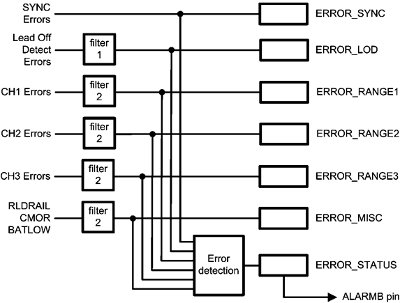 Figure 28. Graphical Illustration of Alarm Propagation
8.3.29 Reference Voltage Generators
The common-mode and right-leg drive reference generates VDD/2.2 volts, which are present on the RLDREF pin. This reference is used as an internal common-mode reference, as the reference for the analog pace channel, and should be powered on at all times when a sigma-delta modulator is running. It can be powered down by programming bit SHDN_CMREF=1 in the REF_CN register. The RLDREF pin should have a 0.1-µF bypass capacitor-to-ground.
The internal reference, VREF, generates 2.4 V, which are present on the CVREF pin. The CVREF pin must have a 1 µF bypass capacitor-to-ground with low ESR and is not designed to be loaded with other circuitry. This reference should also be powered on at all times when a sigma-delta modulator is running. It can be powered down programming bit SHDN_REF=1 in the REF_CN register. It is possible to provide the reference voltage externally on this pin when the internal reference generator is shut down.
All three voltage generators require a somewhat larger start up time compared to the other circuit blocks inside the ADS1293, which is why they are treated differently in the global power-down or standby states, as will be described in the next section.
8.3.30 Power Management
The ADS1293 has many features that allow the optimization of power consumption. The common-mode detector and right-leg drive amplifier can be configured to achieve the optimum AC performance to power consumption ratio in a given application environment. Almost all internal circuit blocks can be powered down to reduce power consumption. Table 7 lists the typical power consumption budget for all of the circuit blocks that can be individually powered down.
There are two master control bits, PWR_DOWN and STANDBY, in addition to the power-down control bits that are used to power-down an individual circuit block, and they are located in the CONFIG register. In the power-down mode, all circuits that can be powered down are powered down, irrespective of the state of their individual shutdown bits. With the PWR_DOWN bit, the entire ADS1293 can be quickly placed in its minimal current consumption state without needing to do many individual configuration register writes. The STANDBY bit operates in a similar manner, but it does not affect the state of the three voltage generators and the crystal oscillator inside the ADS1293, which require a somewhat longer time to start up. When placing the ADS1293 in standby mode, the power consumption is somewhat higher than in the power-down state but the ADS1293 can return to operation quicker. The difference between the current consumption in power-down and in standby depends on the logic state of the shutdown bits of the two reference voltage generators and the crystal oscillator, as described in Table 7.
Table 7 specifies the current consumption of the blocks that are always ON in the first row. The second group in the table specifies the current consumption of the two reference voltage generators and the crystal oscillator that are OFF in power-down mode but that remain active during standby mode. The last group of circuit blocks in the table specifies the current consumption of the other circuit blocks. The ADS1293 will need about 100 ms to return to operation after being powered down. The time to recover from standby is limited by the time latency of the programmable logic filters in the AFE channels, as described in the Filter Settling Time section.
Table 7. Typical Current Consumption Per Block
| GLOBAL POWER CONTROL |
BLOCK NAME | CONDITIONS / NOTES | CURRENT µA |
|---|---|---|---|
| Always on | Supporting circuitry | 80 | |
| Off in power-down | Reference voltage generator | 17 | |
| Right-leg drive reference | 9 | ||
| Crystal oscillator | 7 | ||
| Off in standby | Instrumentation amplifier | low-power, per channel | 38 |
| high-resolution, per channel | 121 | ||
| Analog front end fault detect | Per channel | 2 | |
| Sigma delta modulator | 102.4kHz, per channel | 22 | |
| 204.8kHz, per channel | 41 | ||
| Analog output channel | 29 | ||
| Lead-off detect | Excluding excitation currents | 25 | |
| Wilson reference | per channel | 7 | |
| Common-mode detector | low-speed, cap drive 1, 6 active leads | 39 | |
| high-speed, cap drive 4, 6 active leads | 79 | ||
| Right-leg drive amplifier | low-speed, cap drive 1 | 20 | |
| high-speed, cap drive 4 | 60 |
8.4 Device Functional Modes
A channel can be configured in different modes of operation that allow optimizing for performance and power consumption as required for an application. Further more, the on-chip programmable digital filters provide a range of bandwidth and output data rate configurations that result in different levels of performance.
8.4.1 Low Sampling Rate
The following tables summarize the output data rate, digital filter bandwidth and typical RMS noise of a channel for every decimation ratio combination possible when the sigma-delta modulator is configured for a sampling rate of 102.4 kHz. Table 8 shows the channel parameters when the standard pace data rate is selected, and Table 9 shows the channel parameters when the double pace data rate is selected. The sampling rate of the sigma-delta modulator is selected in the AFE_RES register and the pace data rate is selected in the R1_RATE register.
Table 8. Channel Parameters With SDM Running at 102.4 kHz and at Standard Pace Data Rate (R1 = 4)(1)
| R2 | R3 | PACE CHANNEL | ECG CHANNEL | |||||||
|---|---|---|---|---|---|---|---|---|---|---|
| ADCMAX | ODR [Hz] |
BW [Hz] |
RMS NOISE [mV] |
ADCMAX | ODR [Hz] |
BW [Hz] |
RMS NOISE | |||
| LOW POWER [µV] |
HIGH RES [µV] |
|||||||||
| 4 | 4 | 0x8000 | 6400 | 1300 | 1.612 | 0x800000 | 1600 | 325 | 4.47 | 4.16 |
| 6 | 0xF30000 | 1067 | 215 | 3.42 | 3.05 | |||||
| 8 | 0x800000 | 800 | 160 | 2.92 | 2.57 | |||||
| 12 | 0xF30000 | 533 | 105 | 2.37 | 2.07 | |||||
| 16 | 0x800000 | 400 | 80 | 2.06 | 1.81 | |||||
| 32 | 0x800000 | 200 | 40 | 1.50 | 1.29 | |||||
| 64 | 0x800000 | 100 | 20 | 1.12 | 0.94 | |||||
| 128 | 0x800000 | 50 | 10 | 0.85 | 0.70 | |||||
| 5 | 4 | 0xC350 | 5120 | 1040 | 0.572 | 0xC35000 | 1280 | 260 | 3.82 | 3.42 |
| 6 | 0xB964F0 | 853 | 175 | 3.02 | 2.67 | |||||
| 8 | 0xC35000 | 640 | 130 | 2.60 | 2.29 | |||||
| 12 | 0xB964F0 | 427 | 85 | 2.13 | 1.86 | |||||
| 16 | 0xC35000 | 320 | 65 | 1.86 | 1.62 | |||||
| 32 | 0xC35000 | 160 | 32 | 1.36 | 1.16 | |||||
| 64 | 0xC35000 | 80 | 16 | 1.02 | 0.85 | |||||
| 128 | 0xC35000 | 40 | 8 | 0.79 | 0.64 | |||||
| 6 | 4 | 0xF300 | 4267 | 870 | 0.238 | 0xF30000 | 1067 | 215 | 3.41 | 3.04 |
| 6 | 0xE6A900 | 711 | 145 | 2.74 | 2.42 | |||||
| 8 | 0xF30000 | 533 | 110 | 2.38 | 2.07 | |||||
| 12 | 0xE6A900 | 356 | 70 | 1.96 | 1.70 | |||||
| 16 | 0xF30000 | 267 | 55 | 1.71 | 1.48 | |||||
| 32 | 0xF30000 | 133 | 27 | 1.25 | 1.07 | |||||
| 64 | 0xF30000 | 67 | 13 | 0.94 | 0.79 | |||||
| 128 | 0xF30000 | 33 | 7 | 0.74 | 0.60 | |||||
| 8 | 4 | 0x8000 | 3200 | 650 | 0.060 | 0x800000 | 800 | 160 | 2.91 | 2.58 |
| 6 | 0xF30000 | 533 | 110 | 2.37 | 2.08 | |||||
| 8 | 0x800000 | 400 | 80 | 2.08 | 1.79 | |||||
| 12 | 0xF30000 | 267 | 55 | 1.71 | 1.48 | |||||
| 16 | 0x800000 | 200 | 40 | 1.50 | 1.29 | |||||
| 32 | 0x800000 | 100 | 20 | 1.12 | 0.94 | |||||
| 64 | 0x800000 | 50 | 10 | 0.85 | 0.70 | |||||
| 128 | 0x800000 | 25 | 5 | 0.68 | 0.54 | |||||
Table 9. Channel Parameters With SDM Running at 102.4 kHz and at Double Pace Data Rate (R1 = 2)(1)
| R2 | R3 | PACE CHANNEL | ECG CHANNEL | |||||||
|---|---|---|---|---|---|---|---|---|---|---|
| ADCMAX | ODR [Hz] |
BW [Hz] |
RMS NOISE [mV] |
ADCMAX | ODR [Hz] |
BW [Hz] |
RMS NOISE | |||
| LOW POWER [µV] |
HIGH RES [µV] |
|||||||||
| 4 | 4 | 0x8000 | 12800 | 1280 | 1.479 | 0x800000 | 3200 | 640 | 38.17 | 37.92 |
| 6 | 0xF30000 | 2133 | 430 | 7.04 | 6.72 | |||||
| 8 | 0x800000 | 1600 | 320 | 4.35 | 3.93 | |||||
| 12 | 0xF30000 | 1067 | 215 | 3.40 | 3.02 | |||||
| 16 | 0x800000 | 800 | 160 | 2.92 | 2.57 | |||||
| 32 | 0x800000 | 400 | 80 | 2.08 | 1.79 | |||||
| 64 | 0x800000 | 200 | 40 | 1.49 | 1.29 | |||||
| 128 | 0x800000 | 100 | 20 | 1.11 | 0.93 | |||||
| 5 | 4 | 0xC350 | 10240 | 1030 | 0.540 | 0xC35000 | 2560 | 510 | 12.64 | 12.38 |
| 6 | 0xB964F0 | 1707 | 340 | 4.53 | 4.12 | |||||
| 8 | 0xC35000 | 1280 | 255 | 3.74 | 3.35 | |||||
| 12 | 0xB964F0 | 853 | 170 | 3.01 | 2.65 | |||||
| 16 | 0xC35000 | 640 | 130 | 2.59 | 2.28 | |||||
| 32 | 0xC35000 | 320 | 65 | 1.86 | 1.62 | |||||
| 64 | 0xC35000 | 160 | 32 | 1.36 | 1.16 | |||||
| 128 | 0xC35000 | 80 | 16 | 1.02 | 0.85 | |||||
| 6 | 4 | 0xF300 | 8533 | 860 | 0.228 | 0xF30000 | 2133 | 420 | 6.20 | 5.88 |
| 6 | 0xE6A900 | 1422 | 285 | 3.94 | 3.57 | |||||
| 8 | 0xF30000 | 1067 | 210 | 3.38 | 3.02 | |||||
| 12 | 0xE6A900 | 711 | 140 | 2.74 | 2.42 | |||||
| 16 | 0xF30000 | 533 | 105 | 2.37 | 2.07 | |||||
| 32 | 0xF30000 | 267 | 55 | 1.70 | 1.47 | |||||
| 64 | 0xF30000 | 133 | 26 | 1.26 | 1.07 | |||||
| 128 | 0xF30000 | 67 | 13 | 0.95 | 0.78 | |||||
| 8 | 4 | 0x8000 | 6400 | 650 | 0.058 | 0x800000 | 1600 | 320 | 4.14 | 3.73 |
| 6 | 0xF30000 | 1067 | 215 | 3.35 | 2.96 | |||||
| 8 | 0x800000 | 800 | 160 | 2.89 | 2.54 | |||||
| 12 | 0xF30000 | 533 | 110 | 2.37 | 2.07 | |||||
| 16 | 0x800000 | 400 | 80 | 2.06 | 1.79 | |||||
| 32 | 0x800000 | 200 | 40 | 1.50 | 1.29 | |||||
| 64 | 0x800000 | 100 | 20 | 1.11 | 0.94 | |||||
| 128 | 0x800000 | 50 | 10 | 0.85 | 0.70 | |||||
8.4.2 High Sampling Rate
The following tables summarize the output data rate, digital filter bandwidth and typical RMS noise of a channel for every decimation ratio combination possible when the sigma-delta modulator is configured for a sampling rate of 204.8 kHz. Table 10 shows the channel parameters when the standard pace data rate is selected, and Table 11 shows the channel parameters when the double pace data rate is selected. The sampling rate of the sigma-delta modulator is selected in the AFE_RES register and the pace data rate is selected in the R1_RATE register.
Table 10. Channel Parameters With SDM Running at 204.8 kHz and at Standard Pace Data Rate (R1 = 4)(1)
| R2 | R3 | PACE CHANNEL | ECG CHANNEL | |||||||
|---|---|---|---|---|---|---|---|---|---|---|
| ADCMAX | ODR [Hz] |
BW [Hz] |
RMS NOISE [mV] |
ADCMAX | ODR [Hz] |
BW [Hz] |
RMS NOISE | |||
| LOW POWER [µV] |
HIGH RES [µV] |
|||||||||
| 4 | 4 | 0x8000 | 12800 | 2600 | 1.738 | 0x800000 | 3200 | 640 | 5.20 | 4.59 |
| 6 | 0xF30000 | 2133 | 430 | 3.92 | 3.38 | |||||
| 8 | 0x800000 | 1600 | 325 | 3.32 | 2.86 | |||||
| 12 | 0xF30000 | 1067 | 215 | 2.69 | 2.31 | |||||
| 16 | 0x800000 | 800 | 160 | 2.34 | 1.99 | |||||
| 32 | 0x800000 | 400 | 80 | 1.68 | 1.43 | |||||
| 64 | 0x800000 | 200 | 40 | 1.25 | 1.04 | |||||
| 128 | 0x800000 | 100 | 20 | 0.95 | 0.78 | |||||
| 5 | 4 | 0xC350 | 10240 | 2080 | 0.613 | 0xC35000 | 2560 | 520 | 4.36 | 3.81 |
| 6 | 0xB964F0 | 1707 | 350 | 3.44 | 2.96 | |||||
| 8 | 0xC35000 | 1280 | 260 | 2.95 | 2.54 | |||||
| 12 | 0xB964F0 | 853 | 170 | 2.41 | 2.06 | |||||
| 16 | 0xC35000 | 640 | 130 | 2.10 | 1.79 | |||||
| 32 | 0xC35000 | 320 | 65 | 1.53 | 1.29 | |||||
| 64 | 0xC35000 | 160 | 32 | 1.14 | 0.95 | |||||
| 128 | 0xC35000 | 80 | 15 | 0.88 | 0.72 | |||||
| 6 | 4 | 0xF300 | 8533 | 1740 | 0.256 | 0xF30000 | 2133 | 430 | 3.91 | 3.38 |
| 6 | 0xE6A900 | 1422 | 290 | 3.12 | 2.68 | |||||
| 8 | 0xF30000 | 1067 | 215 | 2.68 | 2.30 | |||||
| 12 | 0xE6A900 | 711 | 140 | 2.21 | 1.88 | |||||
| 16 | 0xF30000 | 533 | 110 | 1.93 | 1.64 | |||||
| 32 | 0xF30000 | 267 | 55 | 1.41 | 1.18 | |||||
| 64 | 0xF30000 | 133 | 27 | 1.06 | 0.88 | |||||
| 128 | 0xF30000 | 67 | 13 | 0.83 | 0.68 | |||||
| 8 | 4 | 0x8000 | 6400 | 1300 | 0.064 | 0x800000 | 1600 | 325 | 3.32 | 2.86 |
| 6 | 0xF30000 | 1067 | 215 | 2.69 | 2.31 | |||||
| 8 | 0x800000 | 800 | 160 | 2.34 | 2.00 | |||||
| 12 | 0xF30000 | 533 | 105 | 1.93 | 1.64 | |||||
| 16 | 0x800000 | 400 | 80 | 1.69 | 1.44 | |||||
| 32 | 0x800000 | 200 | 40 | 1.25 | 1.04 | |||||
| 64 | 0x800000 | 100 | 20 | 0.96 | 0.78 | |||||
| 128 | 0x800000 | 50 | 10 | 0.76 | 0.61 | |||||
Table 11. Channel Parameters With SDM Running at 204.8 kHz and at Double Pace Data Rate (R1 = 2)(1)
| R2 | R3 | PACE CHANNEL | ECG CHANNEL | |||||||
|---|---|---|---|---|---|---|---|---|---|---|
| ADCMAX | ODR [Hz] |
BW [Hz] |
RMS NOISE [mV] |
ADCMAX | ODR [Hz] |
BW [Hz] |
RMS NOISE | |||
| LOW POWER [µV] |
HIGH RES [µV] |
|||||||||
| 4 | 4 | 0x8000 | 25600 | 2550 | 1.592 | 0x800000 | 6400 | 1280 | 41.27 | 40.81 |
| 6 | 0xF30000 | 4267 | 850 | 7.79 | 7.32 | |||||
| 8 | 0x800000 | 3200 | 640 | 4.97 | 4.35 | |||||
| 12 | 0xF30000 | 2133 | 430 | 3.88 | 3.36 | |||||
| 16 | 0x800000 | 1600 | 325 | 3.32 | 2.85 | |||||
| 32 | 0x800000 | 800 | 160 | 2.34 | 1.98 | |||||
| 64 | 0x800000 | 400 | 80 | 1.69 | 1.43 | |||||
| 128 | 0x800000 | 200 | 40 | 1.25 | 1.04 | |||||
| 5 | 4 | 0xC350 | 20480 | 2050 | 0.580 | 0xC35000 | 5120 | 1020 | 13.57 | 13.38 |
| 6 | 0xB964F0 | 3413 | 680 | 5.18 | 4.56 | |||||
| 8 | 0xC35000 | 2560 | 510 | 4.30 | 3.73 | |||||
| 12 | 0xB964F0 | 1707 | 340 | 3.41 | 2.94 | |||||
| 16 | 0xC35000 | 1280 | 260 | 2.94 | 2.53 | |||||
| 32 | 0xC35000 | 640 | 130 | 2.10 | 1.79 | |||||
| 64 | 0xC35000 | 320 | 65 | 1.53 | 1.29 | |||||
| 128 | 0xC35000 | 160 | 32 | 1.14 | 0.95 | |||||
| 6 | 4 | 0xF300 | 17067 | 1720 | 0.245 | 0xF30000 | 4267 | 850 | 6.99 | 6.43 |
| 6 | 0xE6A900 | 2844 | 570 | 4.53 | 3.94 | |||||
| 8 | 0xF30000 | 2133 | 420 | 3.86 | 3.33 | |||||
| 12 | 0xE6A900 | 1422 | 285 | 3.11 | 2.67 | |||||
| 16 | 0xF30000 | 1067 | 215 | 2.69 | 2.29 | |||||
| 32 | 0xF30000 | 533 | 110 | 1.93 | 1.64 | |||||
| 64 | 0xF30000 | 267 | 55 | 1.41 | 1.18 | |||||
| 128 | 0xF30000 | 133 | 26 | 1.06 | 0.88 | |||||
| 8 | 4 | 0x8000 | 12800 | 1300 | 0.062 | 0x800000 | 3200 | 640 | 4.74 | 4.15 |
| 6 | 0xF30000 | 2133 | 425 | 3.82 | 3.28 | |||||
| 8 | 0x800000 | 1600 | 320 | 3.29 | 2.83 | |||||
| 12 | 0xF30000 | 1067 | 215 | 2.68 | 2.30 | |||||
| 16 | 0x800000 | 800 | 160 | 2.34 | 2.00 | |||||
| 32 | 0x800000 | 400 | 80 | 1.69 | 1.42 | |||||
| 64 | 0x800000 | 200 | 40 | 1.25 | 1.05 | |||||
| 128 | 0x800000 | 100 | 20 | 0.95 | 0.79 | |||||
8.4.3 Ouput Code (ADCOUT)
The ADCOUT of the ADS1293 is due to a differential voltage applied between the positive and negative input terminals of the instrumentation amplifier and can be calculated with Equation 13:

The reference voltage VREF, equals to 2.4 V if the on-chip voltage reference is used. ADCMAX represents the maximum output code of the ADC, which corresponds to a theoretical 2.4-V signal at the input of the SDM. The value of ADCMAX changes with the configuration of the digital filters, and the corresponding value can be found in Table 8, Table 9, Table 10, and Table 11. Note that ADCOUT equals ADCMAX/2 for a 0V differential input.
8.5 Programming
8.5.1 Serial Digital Interface
A serial peripheral interface (SPI) allows access to the control registers of the ADS1293. The serial interface is a generic 4-wire synchronous interface compatible with SPI type interfaces used on many microcontrollers and DSP controllers.
8.5.2 Digital Output Drive Strength
The strength of the transistors driving the serial data out pin (SDO) can be programmed to four levels in the DIGO_STRENGTH register. The drive strength will affect the slope of the digital output signal edges, and the optimal drive strength will depend on the capacitive loading on the SDO pin, where larger capacitive loads require larger drive strength. The output drive strength configurability may help reduce interference from the SPI communication into the AFE signal path. In this sense, it is advised to use the lowest drive strength that works for a particular system.
8.5.3 SPI Protocol
A typical serial interface access cycle is exactly 16 bits long, which includes an 8-bit command field (R/WB + 7-bit address) to provide for a maximum of 128 direct access addresses, and an 8-bit data field. Figure 29 shows the access protocol used by this interface. Extended access cycles are possible and they are described in the Auto-Incrementing Address and Streaming sections.
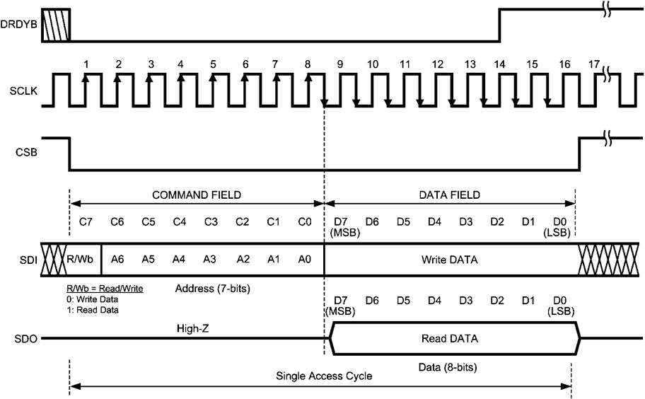 Figure 29. Serial Interface Protocol
Each assertion of chip select bar (CSB) starts a new register access. The R/Wb bit in the command field configures the direction of the access operation; a value of 0 indicates a write operation and a value of 1 indicates a read operation. All output data is driven on the falling edge of the serial clock (SCLK), and for the 16-bit protocol, SDO read data is driven on the falling edge of clocks 8 through 15. All input data on the serial data in (SDI) pin is sampled on the rising edge of SCLK and is written into the register on the rising edge of the 16th clock. The user is required to deassert CSB after the 16th clock; if CSB is deasserted before the 16th clock, no data write will occur.
8.5.4 Random Register Access Protocol
The 16-bit protocol is useful for random address access. CSB must be asserted during 16 clock cycles of SCLK.
8.5.5 Auto-Incrementing Address
An access cycle may be extended to multiple registers by simply keeping the CSB asserted beyond the stated 16 clocks of the standard 16-bit protocol. In this mode, CSB must be asserted during 8*(1+N) clock cycles of SCLK, where N is the amount of bytes to write or read during the access cycle. The auto-incrementing address mode is useful to access a block of registers of incrementing addresses.
For example, to read the pace and ECG data registers located from address 0x30 to address 0x3F and worth 16 bytes of data, follow the next steps:
- Execute a read command to address 0x30.
- Extend the CSB assertion during 136 clock cycles (8+8*16).
During an auto-incrementing read access, SDO outputs the register contents every 8 clock cycles after the initial 8 clocks of the command field. During an auto-incrementing write access, the data is written to the registers every 8 clock cycles after the initial 8 clocks of the command field.
Automatic address increment stops at address 0x4F for both write and read operations.
8.5.6 Streaming
A read access cycle can operate in streaming mode, also referred to as loop read-back mode, by performing a read operation from the DATA_LOOP register and extending the CSB assertion beyond the standard 16 clocks. The streaming mode is supported for the DATA_STATUS, DATA_CH1_PACE, DATA_CH2_PACE, DATA_CH3_PACE, DATA_CH1_ECG, DATA_CH2_ECG and DATA_CH3_ECG registers described in Pace and ECG Data Read Back Registers. The streaming mode is useful to access the block of pace and ECG data registers when not all data needs to be read. The channels to read in this mode are selected in the CH_CNFG register. In this mode, CSB must be asserted during 8*(1+N) clock cycles, where N is the number source bytes enabled in CH_CNFG . The source for pace data is 2 bytes long; the source for ECG data is 3 bytes long, and the source for data status is 1 byte long.
For example, to read the DATA_STATUS, DATA_CH3_PACE and DATA_CH3_ECG registers located at address 0x30, 0x35 and 0x3D and worth 6 bytes of data, follow the next steps:
- Write a value of 0x49 to the CH_CNFG register (address 0x2F).
- Read from the DATA_LOOP register (address 0x50).
- Extend the CSB assertion for 56 clock cycles (8+8*6).
8.5.7 Data Ready Bar
Data ready bar (DRDYB) is an active low-output signal and is asserted when new data is ready to be read. After DRDYB is asserted and an SPI read of ECG or PACE data occurs, DRDYB will be deasserted at the 14th rising edge of SCLK.
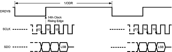 Figure 30. DRDYB Behavior for a Complete Read Operation
New data is available regardless of the serial interface being ready to read the data or not, and therefore, the data is lost if it is not read before the next DRDYB assertion. If DRDYB is asserted and the data is not read, DRDYB is automatically deasserted at least tDRDYB seconds before the next DRDYB assertion. The value for tDRDYB can be found in and .
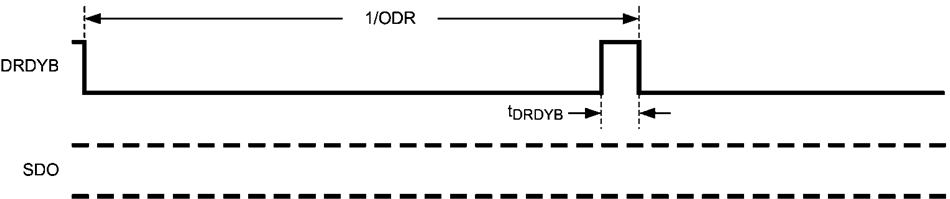 Figure 31. DRDYB Behavior for an Incomplete Read Operation
The source channel driving the assertion of the DRDYB signal can be configured in the DRDYB_SRC register. In order to see the DRDYB output pin asserted, one bit of this register must be set to 1 to select the digital channel to drive it. Multiple channels should not be selected to drive the DRDYB output pin, otherwise, it will result in unexpected behavior. The selected channel should not be shut down in the AFE_SHDN_CN register, and if the source is an ECG channel, its filter should not be disabled in the DIS_EFILTER register. TI strongly recommends selecting the channel with the fastest data rate as the source for the DRDYB signal to avoid loss of data.
By default, the DRDYB signal is masked during the first few data samples after the start of a conversion or when a synchronization error is detected. If any ECG channel is enabled, DRDYB is masked during the first six data samples of the slowest enabled ECG channel. If all ECG channels are disabled, DRDYB is masked for the first six data samples of the slowest enabled pace channel when the data rate is 1xODR, and for the first eleven data samples of the slowest enabled pace channel when the data rate is 2xODR. Masking can be disabled in the MASK_DRDYB register.
8.5.8 Simultaneous ECG and Pace Data Read
Each of the three digital channels of the ADS1293 provides a high-performance path for ECG monitoring and a lower-resolution path for monitoring of pace-maker signals. The digitized signals from these two paths can be read simultaneously from the Pace and ECG Data Read Back Registers.
The ECG signal path achieves higher resolution than the PACE signal path by having one extra filtering stage (as shown in Sinc Filters). Due to the difference in filtering stages of the two paths, the PACE data is available for reading at a much higher rate than the ECG data. In this sense, the PACE channel must be selected as the driving source of the DRDYB signal.
In the Streaming mode, the data from the DATA_LOOP register should be read after the DRDYB line is asserted; this means that new data is available. In order to read both ECG and PACE data from the DATA_LOOP register, the channels of interest must be enabled in the CH_CNFG register.
As an example, the 3-Lead ECG Application can be reconfigured to perform simultaneous ECG and PACE data reads from channel 1:
- Set address 0x00 = 0x00: Stops data conversion (if any).
-
Set address 0x2F = 0x32: Enables channel 1 PACE, channel 1 ECG, and channel 2 ECG for loop.
read-back mode - Set address 0x27 = 0x01: Reconfigures the DRDYB source to channel 1 PACE .
- Set address 0x00 = 0x01: Starts data conversion.
- Set address 0x00 = 0x00: Stops data conversion.
-
Set address 0x2F = 0x33: Enables data ready status, channel 1 PACE, channel 1 ECG, and channel 2.
ECG for loop read-back mode - Set address 0x00 = 0x01: Starts data conversion.
In this case, new PACE data from channel 1 is available on every DRDYB assertion; ECG data from channel 1 and channel 2, on the other hand, is available every six DRDYB assertions (R3_RATE_CH1 = R3_RATE_CH2 = 6).
There are different approaches for handling simultaneous ECG and PACE data read. One approach is to read ECG data every time that PACE data is ready, over-sampling the ECG channel. This is possible because old conversion values are retained in the data registers until new data overwrites them.
A second approach is to also read the DATA_STATUS register. Continuing from the steps above:
The DATA_STATUS register indicates the channel(s) that are updated at a given DRDYB assertion; this information can potentially be used to discard irrelevant data.
A third and more complex approach is to continuously reprogram the CH_CNFG register based on the contents of DATA_STATUS register. The CH_CNFG register should be reprogrammed to read PACE+ECG data only when the DATA_STATUS register indicates ECG data is available. After reading the PACE+ECG data, the CH_CNFG register should be reprogrammed back to reading only the DATA_STATUS register and the PACE data. In this case, the ECG data is not oversampled and the SPI communication can be significantly reduced for cases where a decimation rate, R3_RATE_CHx, is large. The reconfiguration of the CH_CNFG register should be done before the next DRDYB assertion to avoid losing data.
8.6 Register Maps
- If written to, RESERVED bits must be written to 0 unless otherwise indicated.
- Read back value of RESERVED bits and registers is unspecified and should be discarded.
- Recommended values must be programmed and forbidden values must not be programmed where they are indicated in order to avoid unexpected results.
- If written to, registers indicated as Reserved must have the indicated default value as shown in the register map. Any other value can cause unexpected results.
| REGISTER NAME | DESCRIPTION | ADDRESS | ACCESS | DEFAULT |
|---|---|---|---|---|
| Operation Mode Registers | ||||
| CONFIG | Main Configuration | 0x00 | R/W | 0x02 |
| Input Channel Selection Registers | ||||
| FLEX_CH1_CN | Flex Routing Switch Control for Channel 1 | 0x01 | R/W | 0x00 |
| FLEX_CH2_CN | Flex Routing Switch Control for Channel 2 | 0x02 | R/W | 0x00 |
| FLEX_CH3_CN | Flex Routing Switch Control for Channel 3 | 0x03 | R/W | 0x00 |
| FLEX_PACE_CN | Flex Routing Switch Control for Pace Channel | 0x04 | R/W | 0x00 |
| FLEX_VBAT_CN | Flex Routing Switch for Battery Monitoring | 0x05 | R/W | 0x00 |
| Lead-off Detect Control Registers | ||||
| LOD_CN | Lead-Off Detect Control | 0x06 | R/W | 0x08 |
| LOD_EN | Lead-Off Detect Enable | 0x07 | R/W | 0x00 |
| LOD_CURRENT | Lead-Off Detect Current | 0x08 | R/W | 0x00 |
| LOD_AC_CN | AC Lead-Off Detect Control | 0x09 | R/W | 0x00 |
| Common-Mode Detection and Right-Leg Drive Feedback Control Registers | ||||
| CMDET_EN | Common-Mode Detect Enable | 0x0A | R/W | 0x00 |
| CMDET_CN | Common-Mode Detect Control | 0x0B | R/W | 0x00 |
| RLD_CN | Right-Leg Drive Control | 0x0C | R/W | 0x00 |
| Wilson Control Registers | ||||
| WILSON_EN1 | Wilson Reference Input one Selection | 0x0D | R/W | 0x00 |
| WILSON_EN2 | Wilson Reference Input two Selection | 0x0E | R/W | 0x00 |
| WILSON_EN3 | Wilson Reference Input three Selection | 0x0F | R/W | 0x00 |
| WILSON_CN | Wilson Reference Control | 0x10 | R/W | 0x00 |
| Reference Registers | ||||
| REF_CN | Internal Reference Voltage Control | 0x11 | R/W | 0x00 |
| OSC Control Registers | ||||
| OSC_CN | Clock Source and Output Clock Control | 0x12 | R/W | 0x00 |
| AFE Control Registers | ||||
| AFE_RES | Analog Front End Frequency and Resolution | 0x13 | R/W | 0x00 |
| AFE_SHDN_CN | Analog Front End Shutdown Control | 0x14 | R/W | 0x00 |
| AFE_FAULT_CN | Analog Front End Fault Detection Control | 0x15 | R/W | 0x00 |
| RESERVED | — | 0x16 | R/W | 0x00 |
| AFE_PACE_CN | Analog Pace Channel Output Routing Control | 0x17 | R/W | 0x01 |
| Error Status Registers | ||||
| ERROR_LOD | Lead-Off Detect Error Status | 0x18 | RO | — |
| ERROR_STATUS | Other Error Status | 0x19 | RO | — |
| ERROR_RANGE1 | Channel 1 AFE Out-of-Range Status | 0x1A | RO | — |
| ERROR_RANGE2 | Channel 2 AFE Out-of-Range Status | 0x1B | RO | — |
| ERROR_RANGE3 | Channel 3 AFE Out-of-Range Status | 0x1C | RO | — |
| ERROR_SYNC | Synchronization Error | 0x1D | RO | — |
| ERROR_MISC | Miscellaneous Errors | 0x1E | RO | 0x00 |
| Digital Registers | ||||
| DIGO_STRENGTH | Digital Output Drive Strength | 0x1F | R/W | 0x03 |
| R2_RATE | R2 Decimation Rate | 0x21 | R/W | 0x08 |
| R3_RATE_CH1 | R3 Decimation Rate for Channel 1 | 0x22 | R/W | 0x80 |
| R3_RATE_CH2 | R3 Decimation Rate for Channel 2 | 0x23 | R/W | 0x80 |
| R3_RATE_CH3 | R3 Decimation Rate for Channel 3 | 0x24 | R/W | 0x80 |
| R1_RATE | R1 Decimation Rate | 0x25 | R/W | 0x00 |
| DIS_EFILTER | ECG Filter Disable | 0x26 | R/W | 0x00 |
| DRDYB_SRC | Data Ready Pin Source | 0x27 | R/W | 0x00 |
| SYNCB_CN | SYNCB In/Out Pin Control | 0x28 | R/W | 0x40 |
| MASK_DRDYB | Optional Mask Control for DRDYB Output | 0x29 | R/W | 0x00 |
| MASK_ERR | Mask Error on ALARMB Pin | 0x2A | R/W | 0x00 |
| Reserved | — | 0x2B | — | 0x00 |
| Reserved | — | 0x2C | — | 0x00 |
| Reserved | — | 0x2D | — | 0x09 |
| ALARM_FILTER | Digital Filter for Analog Alarm Signals | 0x2E | R/W | 0x33 |
| CH_CNFG | Configure Channel for Loop Read Back Mode | 0x2F | R/W | 0x00 |
| Pace and ECG Data Read Back Registers | ||||
| DATA_STATUS | ECG and Pace Data Ready Status | 0x30 | RO | — |
| DATA_CH1_PACE | Channel 1 Pace Data | 0x31 0x32 |
RO | — |
| DATA_CH2_PACE | Channel 2 Pace Data | 0x33 0x34 |
RO | — |
| DATA_CH3_PACE | Channel 3 Pace Data | 0x35 0x36 |
RO | — |
| DATA_CH1_ECG | Channel 1 ECG Data | 0x37 0x38 0x39 |
RO | — |
| DATA_CH2_ECG | Channel 2 ECG Data | 0x3A 0x3B 0x3C |
RO | — |
| DATA_CH3_ECG | Channel 3 ECG Data | 0x3D 0x3E 0x3F |
RO | — |
| REVID | Revision ID | 0x40 | RO | 0x01 |
| DATA_LOOP | Loop Read-Back Address | 0x50 | RO | — |
8.6.1 Operation Mode Registers
| Addr | 7 | 6 | 5 | 4 | 3 | 2 | 1 | 0 |
|---|---|---|---|---|---|---|---|---|
| 0x00 | PWR_DOWN | STANDBY | START_CON |
| [7:3] | RESERVED | — |
| [2] | PWR_DOWN | Power-down mode |
| 0: Disabled (default) | ||
| 1: Circuit powered down | ||
| [1] | STANDBY | Standby mode |
| 0: Disabled | ||
| 1: Most circuits powered down (default) | ||
| [0] | START_CON | Start conversion |
| 0: Disabled (default) | ||
| 1: Conversion active | ||
| Note: Programming START_CON = 1 locks write access to registers 0x11, 0x12, 0x13 and 0x21–0x29. |
8.6.2 Input Channel Selection Registers
| Addr | 7 | 6 | 5 | 4 | 3 | 2 | 1 | 0 |
|---|---|---|---|---|---|---|---|---|
| 0x01 | TST1 | POS1 | NEG1 | |||||
| [7:6] | TST1 | Test signal selector |
| 00: Test signal disconnected and CH1 inputs determined by POS1 and NEG1 (default) 01: Connect channel one to positive test signal 10: Connect channel one to negative test signal 11: Connect channel one to zero test signal |
||
| [5:3] | POS1 | Positive terminal of channel 1 |
| 000: Positive terminal is disconnected (default) 001: Positive terminal connected to input IN1 010: Positive terminal connected to input IN2 011: Positive terminal connected to input IN3 100: Positive terminal connected to input IN4 101: Positive terminal connected to input IN5 110: Positive terminal connected to input IN6 |
||
| [2:0] | NEG1 | Negative terminal of channel 1 |
| 000: Negative terminal is disconnected (default) 001: Negative terminal connected to input IN1 010: Negative terminal connected to input IN2 011: Negative terminal connected to input IN3 100: Negative terminal connected to input IN4 101: Negative terminal connected to input IN5 110: Negative terminal connected to input IN6 |
| Addr | 7 | 6 | 5 | 4 | 3 | 2 | 1 | 0 |
|---|---|---|---|---|---|---|---|---|
| 0x02 | TST2 | POS2 | NEG2 | |||||
| [7:6] | TST2 | Test signal selector |
| 00: Test signal disconnected and CH2 inputs determined by POS2 and NEG2 (default) 01: Connect channel two to positive test signal 10: Connect channel two to negative test signal 11: Connect channel two to zero test signal |
||
| [5:3] | POS2 | Positive terminal of channel 2 |
| 000: Positive terminal is disconnected (default) 001: Positive terminal connected to input IN1 010: Positive terminal connected to input IN2 011: Positive terminal connected to input IN3 100: Positive terminal connected to input IN4 101: Positive terminal connected to input IN5 110: Positive terminal connected to input IN6 |
||
| [2:0] | NEG2 | Negative terminal of channel 2 |
| 000: Negative terminal is disconnected (default) 001: Negative terminal connected to input IN1 010: Negative terminal connected to input IN2 011: Negative terminal connected to input IN3 100: Negative terminal connected to input IN4 101: Negative terminal connected to input IN5 110: Negative terminal connected to input IN6 |
| Addr | 7 | 6 | 5 | 4 | 3 | 2 | 1 | 0 |
|---|---|---|---|---|---|---|---|---|
| 0x03 | TST3 | POS3 | NEG3 | |||||
| [7:6] | TST3 | Test signal selector |
| 00: Test signal disconnected and CH3 inputs determined by POS3 and NEG3 (default) 01: Connect channel three to positive test signal 10: Connect channel three to negative test signal 11: Connect channel three to zero test signal |
||
| [5:3] | POS3 | Positive terminal of channel 3 |
| 000: Positive terminal is disconnected (default) 001: Positive terminal connected to input IN1 010: Positive terminal connected to input IN2 011: Positive terminal connected to input IN3 100: Positive terminal connected to input IN4 101: Positive terminal connected to input IN5 110: Positive terminal connected to input IN6 |
||
| [2:0] | NEG3 | Negative terminal of channel 3 |
| 000: Negative terminal is disconnected (default) 001: Negative terminal connected to input IN1 010: Negative terminal connected to input IN2 011: Negative terminal connected to input IN3 100: Negative terminal connected to input IN4 101: Negative terminal connected to input IN5 110: Negative terminal connected to input IN6 |
| Addr | 7 | 6 | 5 | 4 | 3 | 2 | 1 | 0 |
|---|---|---|---|---|---|---|---|---|
| 0x04 | TST4 | POS4 | NEG4 | |||||
| [7:6] | TST4 | Test signal selector |
| 00: Test signal disconnected and PACE inputs determined by POS4 and NEG4 (default) 01: Connect pace channel to positive test signal 10: Connect pace channel to negative test signal 11: Connect pace channel to zero test signal |
||
| [5:3] | POS4 | Positive terminal of pace channel |
| 000: Positive terminal is disconnected (default) 001: Positive terminal connected to input IN1 010: Positive terminal connected to input IN2 011: Positive terminal connected to input IN3 100: Positive terminal connected to input IN4 101: Positive terminal connected to input IN5 110: Positive terminal connected to input IN6 |
||
| [2:0] | NEG4 | Negative terminal of pace channel |
| 000: Negative terminal is disconnected (default) 001: Negative terminal connected to input IN1 010: Negative terminal connected to input IN2 011: Negative terminal connected to input IN3 100: Negative terminal connected to input IN4 101: Negative terminal connected to input IN5 110: Negative terminal connected to input IN6 |
| Addr | 7 | 6 | 5 | 4 | 3 | 2 | 1 | 0 |
|---|---|---|---|---|---|---|---|---|
| 0x05 | VBAT_ MONI_CH3 | VBAT_ MONI_CH2 | VBAT_ MONI_CH1 |
| [7:3] | RESERVED | — |
| [2] | VBAT_MONI_CH3 | Battery monitor configuration for channel 3 |
| 0: Battery voltage monitor disabled (default) 1: Battery voltage monitor enabled and overrides FLEX_CH3_CN register |
||
| [1] | VBAT_MONI_CH2 | Battery monitor configuration for channel 2 |
| 0: Battery voltage monitor disabled (default) 1: Battery voltage monitor enabled and overrides FLEX_CH2_CN register |
||
| [0] | VBAT_MONI_CH1 | Battery monitor configuration for channel 1 |
| 0: Battery voltage monitor disabled (default) 1: Battery voltage monitor enabled and overrides FLEX_CH1_CN register |
||
| Note: The INA of the corresponding monitoring channel must be shut down in 0x14. | ||
8.6.3 Lead-Off Detect Control Registers
| Addr | 7 | 6 | 5 | 4 | 3 | 2 | 1 | 0 |
|---|---|---|---|---|---|---|---|---|
| 0x06 | ACAD_LOD | SHDN_LOD | SELAC_LOD | ACLVL_LOD | ||||
| [7:5] | RESERVED | — |
| [4] | ACAD_LOD | AC analog/digital lead-off mode select |
| 0: Digital AC lead-off detect (default) 1: Analog AC lead-off detect |
||
| [3] | SHDN_LOD | Shut down lead-off detection |
| 0: Lead-off detection circuitry is active 1: Lead-off detection circuitry is shut down (default) |
||
| [2] | SELAC_LOD | Lead-off detect operation mode |
| 0: DC lead-off mode (default) 1: AC lead-off mode |
||
| [1:0] | ACLVL_LOD | Programmable comparator trigger level for AC lead-off detection |
| 00: Level 1 (default) 01: Level 2 10: Level 3 11: Level 4 |
| Addr | 7 | 6 | 5 | 4 | 3 | 2 | 1 | 0 |
|---|---|---|---|---|---|---|---|---|
| 0x07 | EN_LOD | |||||||
| [7:6] | RESERVED | — |
| [5] | EN_LOD_6 | DC or Analog AC Lead-off-Detection:
These bits enable the lead-off-detection for input IN6. 0: Lead-off detection disabled (default) 1: Lead-off detection enabled |
| Digital AC Lead-off-Detection:
These bits configure the phase of the current injected into channel CH3. 0: In-phase (default) 1: Anti-phase |
||
| [4] | EN_LOD_5 | DC or Analog AC Lead-off-Detection:
These bits enable the lead-off-detection for input IN5. 0: Lead-off detection disabled (default) 1: Lead-off detection enabled |
| Digital AC Lead-off-Detection:
These bits configure the phase of the current injected into channel CH2. 0: In-phase (default) 1: Anti-phase |
||
| [3] | EN_LOD_4 | DC or Analog AC Lead-off-Detection:
These bits enable the lead-off-detection for input IN4. 0: Lead-off detection disabled (default) 1: Lead-off detection enabled |
| Digital AC Lead-off-Detection:
These bits configure the phase of the current injected into channel CH1. 0: In-phase (default) 1: Anti-phase |
||
| [2] | EN_LOD_3 | DC or Analog AC Lead-off-Detection:
These bits enable the lead-off-detection for input IN3. 0: Lead-off detection disabled (default) 1: Lead-off detection enabled |
| Digital AC Lead-off-Detection:
These bits enable the lead-off-detection for channel CH3. 0: Lead-off detection disabled (default) 1: Lead-off detection enabled |
||
| [1] | EN_LOD_2 | DC or Analog AC Lead-off-Detection:
These bits enable the lead-off-detection for input IN2. 0: Lead-off detection disabled (default) 1: Lead-off detection enable |
| Digital AC Lead-off-Detection:
These bits enable the lead-off-detection for channel CH2. 0: Lead-off detection disabled (default) 1: Lead-off detection enabled |
||
| [0] | EN_LOD_1 | DC or Analog AC Lead-off-Detection:
These bits enable the lead-off-detection for input IN1. 0: Lead-off detection disabled (default) 1: Lead-off detection enable |
| Digital AC Lead-off-Detection:
These bits enable the lead-off-detection for channel CH1. 0: Lead-off detection disabled (default) 1: Lead-off detection enabled |
| Addr | 7 | 6 | 5 | 4 | 3 | 2 | 1 | 0 |
|---|---|---|---|---|---|---|---|---|
| 0x08 | CUR_LOD | |||||||
| [7:0] | CUR_LOD | Lead-off detect current select |
| The lead-off detect current is programmable in a range of 2.04μA with steps of 8nA. 00000000: 0.000 μA (default) 00000001: 0.008 μA . . . . 11111110: 2.032 μA 11111111: 2.040 μA |
| Addr | 7 | 6 | 5 | 4 | 3 | 2 | 1 | 0 |
|---|---|---|---|---|---|---|---|---|
| 0x09 | ACDIV_ FACTOR | ACDIV_LOD | ||||||
| [7] | ACDIV_FACTOR | AC lead off test frequency division factor |
| 0: Clock divider factor K = 1 (default) 1: Clock divider factor K = 16 |
||
| [6:0] | ACDIV_LOD | Clock divider ratiio for AC lead off |
| There are 7 bits available to program the clock divider that generates the AC lead off test frequency. |
8.6.4 Common-Mode Detection and Right-Leg Drive Common-Mode Feedback Control Registers
| Addr | 7 | 6 | 5 | 4 | 3 | 2 | 1 | 0 |
|---|---|---|---|---|---|---|---|---|
| 0x0A | CMDET_ EN_IN6 | CMDET_ EN_IN5 | CMDET_ EN_IN4 | CMDET_ EN_IN3 | CMDET_ EN_IN2 | CMDET_ EN_IN1 |
| [7:6] | RESERVED | — |
| [5:0] | CMDET_EN_INx | Common-mode detect input enable |
| There is one bit available per input pin, where the MSB corresponds to input pin IN6 and the LSB corresponds to input pin IN1. 0: Disable (default) 1: Enable the corresponding pin's voltage to contribute to the average voltage of the common-mode detect block. |
| Addr | 7 | 6 | 5 | 4 | 3 | 2 | 1 | 0 |
|---|---|---|---|---|---|---|---|---|
| 0x0B | CMDET_BW | CMDET_CAPDRIVE | ||||||
| [7:6] | RESERVED | — |
| [2] | CMDET_BW | Common-mode detect bandwidth mode |
| 0: Low-bandwidth mode (default) 1: High-bandwidth mode |
||
| [1:0] | CMDET_CAPDRIVE | Common-mode detect capacitive load drive capability |
| 00: Low cap-drive mode (default) 01: Medium low cap-drive mode 10: Medium high cap-drive mode 11: High cap-drive mode |
| Addr | 7 | 6 | 5 | 4 | 3 | 2 | 1 | 0 |
|---|---|---|---|---|---|---|---|---|
| 0x0C | RLD_BW | RLD_CAPDRIVE | SHDN_RLD | SELRLD | ||||
| [7] | RESERVED | — |
| [6] | RLD_BW | Right-leg drive bandwidth mode |
| 0: Low-bandwidth mode (default) 1: High-bandwidth mode |
||
| [5:4] | RLD_CAPDRIVE | Right-leg drive capacitive load drive capability |
| 00: Low cap-drive mode (default) 01: Medium low cap-drive mode 10: Medium high cap-drive mode 11: High cap-drive mode |
||
| [3] | SHDN_RLD | Shut down right-leg drive amplifier |
| 0: RLD amplifier powered up (default) 1: RLD amplifier powered down |
||
| [2:0] | SELRLD | Right-leg drive multiplexer |
| 000: Right-leg drive output disconnected (default) 001: Right-leg drive output connected to IN1 010: Right-leg drive output connected to IN2 011: Right-leg drive output connected to IN3 100: Right-leg drive output connected to IN4 101: Right-leg drive output connected to IN5 110: Right-leg drive output connected to IN6 |
8.6.5 Wilson Control Registers
| Addr | 7 | 6 | 5 | 4 | 3 | 2 | 1 | 0 |
|---|---|---|---|---|---|---|---|---|
| 0x0D | SELWILSON1 | |||||||
| [7] | RESERVED | — |
| [2:0] | SELWILSON1 | Wilson reference routing for the first buffer amplifier |
| 000: No connection to the first buffer amplifier (default) 001: First buffer amplifier connected to input IN1 010: First buffer amplifier connected to input IN2 011: First buffer amplifier connected to input IN3 100: First buffer amplifier connected to input IN4 101: First buffer amplifier connected to input IN5 110: First buffer amplifier connected to input IN6 |
| Addr | 7 | 6 | 5 | 4 | 3 | 2 | 1 | 0 |
|---|---|---|---|---|---|---|---|---|
| 0x0E | SELWILSON2 | |||||||
| [7:3] | RESERVED | — |
| [2:0] | SELWILSON2 | Wilson reference routing for the second buffer amplifier |
| 000: No connection to the second buffer amplifier (default) 001: Second buffer amplifier connected to input IN1 010: Second buffer amplifier connected to input IN2 011: Second buffer amplifier connected to input IN3 100: Second buffer amplifier connected to input IN4 101: Second buffer amplifier connected to input IN5 110: Second buffer amplifier connected to input IN6 |
| Addr | 7 | 6 | 5 | 4 | 3 | 2 | 1 | 0 |
|---|---|---|---|---|---|---|---|---|
| 0x0F | SELWILSON3 | |||||||
| [7:3] | RESERVED | — |
| [2:0] | SELWILSON3 | Wilson reference routing for the third buffer amplifier |
| 000: No connection to the third buffer amplifier (default) 001: Third buffer amplifier connected to input IN1 010: Third buffer amplifier connected to input IN2 011: Third buffer amplifier connected to input IN3 100: Third buffer amplifier connected to input IN4 101: Third buffer amplifier connected to input IN5 110: Third buffer amplifier connected to input IN6 |
| Addr | 7 | 6 | 5 | 4 | 3 | 2 | 1 | 0 |
|---|---|---|---|---|---|---|---|---|
| 0x10 | GOLDINT | WILSONINT |
| [7:2] | RESERVED | — |
| [1] | GOLDINT | Goldberger reference routing |
| 0: Goldberger reference disabled (default) 1: Goldberger reference outputs internally connected to IN4, IN5 and IN6 Note: GOLDINT bit can not be 1 when WILSONINT is 1. |
||
| [0] | WILSONINT | Wilson reference routing |
| 0: Wilson reference output internally disconnected from IN6 (default) 1: Wilson reference output internally connected to IN6 Note: WILSONINT bit can not be 1 when GOLDINT is 1. |
8.6.6 Reference Registers
| Addr | 7 | 6 | 5 | 4 | 3 | 2 | 1 | 0 |
|---|---|---|---|---|---|---|---|---|
| 0x11 | SHDN_ CMREF | SHDN_REF |
| [7:2] | RESERVED | — |
| [1] | SHDN_CMREF | Shut down the common-mode and right-leg drive reference voltage circuitry |
| 0: CM and RLD reference voltage is on (default) 1: Shut down CM and RLD reference voltage Note: Enable this bit to save power when the analog block is shut down (SHDN_REF = 1). Power-down mode automatically shuts down the common-mode and right-leg drive reference. |
||
| [0] | SHDN_REF | Shut down internal 2.4-V reference voltage |
| 0: Internal reference voltage is on (default) 1: Shut down internal reference voltage Note: Enabling this bit allows driving the IC with an external reference voltage on the CVREF pin. Power-down mode automatically shuts down the internal 2.4-V reference. |
8.6.7 OSC Control Registers
| Addr | 7 | 6 | 5 | 4 | 3 | 2 | 1 | 0 |
|---|---|---|---|---|---|---|---|---|
| 0x12 | STRTCLK | SHDN_OSC | EN_CLKOUT |
| [7:3] | RESERVED | — |
| [2] | STRTCLK | Start the clock |
| 0: Clock to digital disabled (default) 1: Enable clock to digital Note: Set this bit high only after the oscillator has started up or after the oscillator has shut down and the external clock has started up. |
||
| [1] | SHDN_OSC | Select clock source |
| 0: Use internal clock with external crystal on XTAL1 and XTAL2 pins (default) 1: Shut down internal oscillator and use external clock from CLK pin Note: STRTCLK bit should be low at the time this bit is reconfigured. |
||
| [0] | EN_CLKOUT | Enable CLK pin output driver |
| 0: Clock output driver disabled (default) 1: Clock output driver enabled |
8.6.8 AFE Control Registers
| Addr | 7 | 6 | 5 | 4 | 3 | 2 | 1 | 0 |
|---|---|---|---|---|---|---|---|---|
| 0x13 | FS_HIGH_ CH3 |
FS_HIGH_ CH2 |
FS_HIGH_ CH1 |
EN_HIRES_ CH3 |
EN_HIRES_ CH2 |
EN_HIRES_ CH1 |
| [7:6] | RESERVED | — |
| [5] | FS_HIGH_CH3 | Clock frequency for channel 3 |
| 0: 102400 Hz (default) 1: 204800 Hz |
||
| [4 ] | FS_HIGH_CH2 | Clock frequency for Channel 2 |
| 0: 102400 Hz (default) 1: 204800 Hz |
||
| [3] | FS_HIGH_CH1 | Clock frequency for Channel 1 |
| 0: 102400 Hz (default) 1: 204800 Hz |
||
| [2] | EN_HIRES_CH3 | High-resolution mode for Channel 3 instrumentation amplifier |
| 0: Disabled (default) 1: Enabled |
||
| [1] | EN_HIRES_CH2 | High-resolution mode for Channel 2 instrumentation amplifier |
| 0: Disabled (default) 1: Enabled |
||
| [0] | EN_HIRES_CH1 | High-resolution mode for Channel 1 instrumentation amplifier |
| 0: Disabled (default) 1: Enabled |
| Addr | 7 | 6 | 5 | 4 | 3 | 2 | 1 | 0 |
|---|---|---|---|---|---|---|---|---|
| 0x14 | SHDN_ SDM_CH3 |
SHDN_ SDM_CH2 |
SHDN_ SDM_CH1 |
SHDN_ INA_CH3 |
SHDN_ INA_CH2 |
SHDN_ INA_CH1 |
| [7:6] | RESERVED | — |
| [5] | SHDN_SDM_CH3 | Shut down the sigma-delta modulator for Channel 3 |
| 0: Active (default) 1: Shut down |
||
| [4 ] | SHDN_SDM_CH2 | Shut down the sigma-delta modulator for Channel 2 |
| 0: Active (default) 1: Shut down |
||
| [3] | SHDN_SDM_CH1 | Shut down the sigma-delta modulator for Channel 1 |
| 0: Active (default) 1: Shut down |
||
| [2] | SHDN_INA_CH3 | Shut down the instrumentation amplifier for Channel 3 |
| 0: Active (default) 1: Shut down |
||
| [1] | SHDN_INA_CH2 | Shut down the instrumentation amplifier for Channel 2 |
| 0: Active (default) 1: Shut down |
||
| [0] | SHDN_INA_CH1 | Shut down the instrumentation amplifier for Channel 1 |
| 0: Active (default) 1: Shut down |
| Addr | 7 | 6 | 5 | 4 | 3 | 2 | 1 | 0 |
|---|---|---|---|---|---|---|---|---|
| 0x15 | SHDN_ FAULTDET_ CH3 |
SHDN_ FAULTDET_ CH2 |
SHDN_ FAULTDET_ CH1 |
| [7:3] | RESERVED | — |
| [2] | SHDN_
FAULTDET_CH3 |
Disable the instrumentation amplifier fault detection for Channel 3 |
| 0: Fault detection active (default) 1: Disable the fault detection |
||
| [1 ] | SHDN_
FAULTDET_CH2 |
Disable the instrumentation amplifier fault detection for Channel 2 |
| 0: Active (default) 1: Disable the fault detection |
||
| [0] | SHDN_
FAULTDET_CH1 |
Disable the instrumentation amplifier fault detection for Channel 1 |
| 0: Active (default) 1: Disable the fault detection |
| Addr | 7 | 6 | 5 | 4 | 3 | 2 | 1 | 0 |
|---|---|---|---|---|---|---|---|---|
| 0x17 | PACE2RLDIN | PACE2WCT | SHDN_PACE |
| [7:3] | RESERVED | — |
| [2] | PACE2RLDIN | Connect the analog pace channel output to RLDIN pin |
| 0: Analog pace channel output is disconnected from the RLDIN pin (default) 1: Connect the analog pace channel output to the RLDIN pin. Note: The right-leg drive amplifier is disconnected from the RLDIN pin and connected internally to the RLDREF pin when this bit is 1. |
||
| [1 ] | PACE2WCT | Connect the analog pace channel output to WCT pin |
| 0: Analog pace channel output is disconnected from the WCT pin (default) 1: Connect the analog pace channel output to the WCT pin. Note: The Wilson reference output is disconnected from the WCT pin when this bit is 1. The Wilson output can be connected internally to IN6 pin with the WILSON_CN register. |
||
| [0] | SHDN_PACE | Shut down analog pace channel |
| 0: Analog pace channel is powered up 1: Analog pace channel is shut down (default) |
8.6.9 Error Status Registers
| Addr | 7 | 6 | 5 | 4 | 3 | 2 | 1 | 0 |
|---|---|---|---|---|---|---|---|---|
| 0x18 | OUT_LOD | |||||||
| [7:6] | RESERVED | — |
| [5:0] | OUT_LOD | Lead-Off Detect Status |
| There is one bit available per input pin, where the MSB corresponds to input pin IN6 and the LSB corresponds to input pin IN1. 1: Indicates a lead off error detected on the corresponding input pin. |
||
| Note: The clock-to-digital (internal or external) must be enabled in 0x12[2] for this error register to update. | ||
| Addr | 7 | 6 | 5 | 4 | 3 | 2 | 1 | 0 |
|---|---|---|---|---|---|---|---|---|
| 0x19 | SYNC EDGEERR | CH3ERR | CH2ERR | CH1ERR | LEADOFF | BATLOW | RLDRAIL | CMOR |
| [7] | SYNCEDGEERR | Digital synchronization error |
| 1: Indicates a digital synchronization error occurred | ||
| [6] | CH3ERR | Channel 3 out-of-range error |
| 1: Indicates an out-of-range error detected on Channel 3 | ||
| [5] | CH2ERR | Channel 2 out-of-range error |
| 1: Indicates an out-of-range error detected on Channel 2 | ||
| [4 ] | CH1ERR | Channel 1 out-of-range error |
| 1: Indicates an out-of-range error detected on Channel 1 | ||
| [3] | LEADOFF | Lead off detected |
| 1: Indicates a lead off was detected on at least one input pin | ||
| [2] | BATLOW | Low battery |
| 1: Indicates the battery voltage has dropped below 2.7 V | ||
| [1] | RLDRAIL | Right leg drive near rail |
| 1: Indicates the right leg drive amplifier output is approaching the supply rails | ||
| [0] | CMOR | Common-mode level out-of-range |
| 1: Indicates the level detected by the common-mode detect block is outside of the input common-mode range of the amplifiers in the analog front-end | ||
| Note: The clock to digital (internal or external) must be enabled in 0x12[2] for this error register to update. | ||
| Addr | 7 | 6 | 5 | 4 | 3 | 2 | 1 | 0 |
|---|---|---|---|---|---|---|---|---|
| 0x1A | SDM_ OR_CH1 | SIGN_CH1 | OUTN_ LOW_CH1 | OUTN_ HIGH_CH1 | OUTP_ LOW_CH1 | OUTP_ HIGH_CH1 | DIF_HIGH_ CH1 |
| [7] | RESERVED | — |
| [6] | SDM_OR_CH1 | Channel 1 sigma-delta modulator over range |
| 1: Indicates an over range detected for Channel 1 SDM | ||
| [5] | SIGN_CH1 | Channel 1 instrumentation amplifier output sign |
| This bit specifies the sign of the output signal of the instrumentation amplifier for Channel 1. 0: Positive output of INA larger than negative output 1: Positive output of INA smaller than negative output |
||
| [4 ] | OUTN_LOW_CH1 | Channel 1 instrumentation amplifier negative output near negative rail |
| 1: Indicates the negative output of the INA is close to the negative rail for Channel 1 | ||
| [3] | OUTN_HIGH_CH1 | Channel 1 instrumentation amplifier negative output near positive rail |
| 1: Indicates the negative output of the INA is close to the positive rail for Channel 1 | ||
| [2] | OUTP_LOW_CH1 | Channel 1 instrumentation amplifier positive output near negative rail |
| 1: Indicates the positive output of the INA is close to the negative rail for Channel 1 | ||
| [1] | OUTP_HIGH_CH1 | Channel 1 instrumentation amplifier positive output near positive rail |
| 1: Indicates the positive output of the INA is close to the positive rail for Channel 1 | ||
| [0] | DIF_HIGH_CH1 | Channel 1 instrumentation amplifier output out-of-range |
| 1: Indicates the differential output voltage of the INA is out-of-range for Channel 1 | ||
| Note: The clock-to-digital (internal or external) must be enabled in 0x12[2] for this error register to update. | ||
| Addr | 7 | 6 | 5 | 4 | 3 | 2 | 1 | 0 |
|---|---|---|---|---|---|---|---|---|
| 0x1B | SDM_ OR_CH2 | SIGN_CH2 | OUTN_ LOW_CH2 | OUTN_ HIGH_CH2 | OUTP_ LOW_CH2 | OUTP_ HIGH_CH2 | DIF_HIGH_ CH2 |
| [7] | RESERVED | — |
| [6] | SDM_OR_CH2 | Channel 2 sigma-delta modulator over range |
| 1: Indicates an over range detected for channel 2 SDM | ||
| [5] | SIGN_CH2 | Channel 2 instrumentation amplifier output sign |
| This bit specifies the sign of the output signal of the instrumentation amplifier for Channel 2. 0: Positive output of INA larger than negative output 1: Positive output of INA smaller than negative output |
||
| [4 ] | OUTN_LOW_CH2 | Channel 2 instrumentation amplifier negative output near negative rail |
| 1: Indicates the negative output of the INA is close to the negative rail for Channel 2 | ||
| [3] | OUTN_HIGH_CH2 | Channel 2 instrumentation amplifier negative output near positive rail |
| 1: Indicates the negative output of the INA is close to the positive rail for Channel 2 | ||
| [2] | OUTP_LOW_CH2 | Channel 2 instrumentation amplifier positive output near negative rail |
| 1: Indicates the positive output of the INA is close to the negative rail for Channel 2 | ||
| [1] | OUTP_HIGH_CH2 | Channel 2 instrumentation amplifier positive output near positive rail |
| 1: Indicates the positive output of the INA is close to the positive rail for Channel 2 | ||
| [0] | DIF_HIGH_CH2 | Channel 2 instrumentation amplifier output out-of-range |
| 1: Indicates the differential output voltage of the INA is out-of-range for Channel 2 | ||
| Note: The clock-to-digital (internal or external) must be enabled in 0x12[2] for this error register to update. | ||
| Addr | 7 | 6 | 5 | 4 | 3 | 2 | 1 | 0 |
|---|---|---|---|---|---|---|---|---|
| 0x1C | SDM_ OR_CH3 | SIGN_CH3 | OUTN_ LOW_CH3 | OUTN_ HIGH_CH3 | OUTP_ LOW_CH3 | OUTP_ HIGH_CH3 | DIF_HIGH_ CH3 |
| [7] | RESERVED | — |
| [6] | SDM_OR_CH3 | Channel 3 sigma-delta modulator over range |
| 1: Indicates an over range detected for channel 3 SDM | ||
| [5] | SIGN_CH3 | Channel 3 instrumentation amplifier output sign |
| This bit specifies the sign of the output signal of the instrumentation amplifier for Channel 3. 0: Positive output of INA larger than negative output 1: Positive output of INA smaller than negative output |
||
| [4 ] | OUTN_LOW_CH3 | Channel 3 instrumentation amplifier negative output near negative rail |
| 1: Indicates the negative output of the INA is close to the negative rail for Channel 3 | ||
| [3] | OUTN_HIGH_CH3 | Channel 3 instrumentation amplifier negative output near positive rail |
| 1: Indicates the negative output of the INA is close to the positive rail for Channel 3 | ||
| [2] | OUTP_LOW_CH3 | Channel 3 instrumentation amplifier positive output near negative rail |
| 1: Indicates the positive output of the INA is close to the negative rail for Channel 3 | ||
| [1] | OUTP_HIGH_CH3 | Channel 3 instrumentation amplifier positive output near positive rail |
| 1: Indicates the positive output of the INA is close to the positive rail for Channel 3 | ||
| [0] | DIF_HIGH_CH3 | Channel 3 instrumentation amplifier output out-of-range |
| 1: Indicates the differential output voltage of the INA is out-of-range for Channel 3 | ||
| Note: The clock-to-digital (internal or external) must be enabled in 0x12[2] for this error register to update. | ||
| Addr | 7 | 6 | 5 | 4 | 3 | 2 | 1 | 0 |
|---|---|---|---|---|---|---|---|---|
| 0x1D | SYNC_PHASEERR | SYNC_ CH3ERR | SYNC_ CH2ERR | SYNC_ CH1ERR |
| [7:4] | RESERVED | — |
| [3] | SYNC_PHASEERR | Clock timing generator phase error |
| 1: Timing generator phase adjusted to comply with SYNCB signal | ||
| [2] | SYNC_CH3ERR | Channel 3 synchronization error |
| 1: Channel's filter timing updated to comply with synchronization source | ||
| [1] | SYNC_CH2ERR | Channel 2 synchronization error |
| 1: Channel's filter timing updated to comply with synchronization source | ||
| [0] | SYNC_CH1ERR | Channel 1 synchronization error |
| 1: Channel's filter timing updated to comply with synchronization source |
| Addr | 7 | 6 | 5 | 4 | 3 | 2 | 1 | 0 |
|---|---|---|---|---|---|---|---|---|
| 0x1E | BATLOW_ STATUS | RLDRAIL_ STATUS | CMOR_ STATUS |
| [7:3] | RESERVED | — |
| [2] | BATLOW_STATUS | Low-battery error status |
| 1: Indicates the battery voltage has dropped below 2.7 V | ||
| [1] | RLDRAIL_STATUS | Right-leg drive near rail error status |
| 1: Indicates the right leg drive amplifier output is approaching the supply rails | ||
| [0] | CMOR_STATUS | Common-mode level out-of-range error status |
| 1: Indicates the level detected by the common-mode detect block is outside of the input common-mode range of the amplifiers in the analog front end | ||
| Note: The clock-to-digital (internal or external) must be enabled in 0x12[2] for this error register to update. | ||
8.6.10 Digital Registers
| Addr | 7 | 6 | 5 | 4 | 3 | 2 | 1 | 0 |
|---|---|---|---|---|---|---|---|---|
| 0x1F | DIGO_STRENGTH | |||||||
| [7:2] | RESERVED | — |
| [1:0] | DIGO_STRENGTH | Digital Output Drive Strength |
| 00: Low drive mode 01: Mid-low drive mode 10: Mid-high drive mode 11: High drive mode (Default) |
| Addr | 7 | 6 | 5 | 4 | 3 | 2 | 1 | 0 |
|---|---|---|---|---|---|---|---|---|
| 0x21 | R2_RATE | |||||||
| [7:4] | RESERVED | — |
| [3:0] | R2_RATE | R2 decimation rate |
| 0001: 4 0010: 5 0100: 6 1000: 8 (default) Note: The register sets to its default value if none or more than one bit are enabled. |
| Addr | 7 | 6 | 5 | 4 | 3 | 2 | 1 | 0 |
|---|---|---|---|---|---|---|---|---|
| 0x22 | R3_RATE_CH1 | |||||||
| [7:0] | R3_RATE_CH1 | R3 decimation rate for channel 1 |
| 00000001: 4 00000010: 6 00000100: 8 00001000: 12 00010000: 16 00100000: 32 01000000: 64 10000000: 128 (default) Note: The register sets to its default value if none or more than one bit are enabled. |
| Addr | 7 | 6 | 5 | 4 | 3 | 2 | 1 | 0 |
|---|---|---|---|---|---|---|---|---|
| 0x23 | R3_RATE_CH2 | |||||||
| [7:0] | R3_RATE_CH2 | R3 decimation rate for channel 2 |
| 00000001: 4 00000010: 6 00000100: 8 00001000: 12 00010000: 16 00100000: 32 01000000: 64 10000000: 128 (default) Note: The register sets to its default value if none or more than one bit are enabled. |
| Addr | 7 | 6 | 5 | 4 | 3 | 2 | 1 | 0 |
|---|---|---|---|---|---|---|---|---|
| 0x24 | R3_RATE_CH3 | |||||||
| [7:0] | R3_RATE_CH3 | R3 decimation rate for channel 3 |
| 00000001: 4 00000010: 6 00000100: 8 00001000: 12 00010000: 16 00100000: 32 01000000: 64 10000000: 128 (default) Note: The register sets to its default value if none or more than one bit are enabled. |
| Addr | 7 | 6 | 5 | 4 | 3 | 2 | 1 | 0 |
|---|---|---|---|---|---|---|---|---|
| 0x25 | R1_RATE_ CH3 |
R1_RATE_ CH2 |
R1_RATE_ CH1 |
| [7:3] | RESERVED | — |
| [2] | R1_RATE_CH3 | Pace data rate for channel 3 |
| 0: R1 = 4: Standard PACE Data Rate (default) 1: R1 = 2: Double PACE Data Rate |
||
| [1] | R1_RATE_CH2 | Pace data rate for channel 2 |
| 0: R1 = 4: Standard PACE Data Rate (default) 1: R1 = 2: Double PACE Data Rate |
||
| [0] | R1_RATE_CH1 | Pace data rate for channel 1 |
| 0: R1 = 4: Standard PACE Data Rate (default) 1: R1 = 2: Double PACE Data Rate |
| Addr | 7 | 6 | 5 | 4 | 3 | 2 | 1 | 0 |
|---|---|---|---|---|---|---|---|---|
| 0x26 | DIS_E3 | DIS_E2 | DIS_E1 |
| [7:3] | RESERVED | — |
| [2] | DIS_E3 | Disable the ECG filter for channel 3 |
| 0: ECG filter enabled (default) 1: ECG filter disabled |
||
| [1] | DIS_E2 | Disable the ECG filter for channel 2 |
| 0: ECG filter enabled (default) 1: ECG filter disabled |
||
| [0] | DIS_E1 | Disable the ECG filter for channel 1 |
| 0: ECG filter enabled (default) 1: ECG filter disabled |
| Addr | 7 | 6 | 5 | 4 | 3 | 2 | 1 | 0 |
|---|---|---|---|---|---|---|---|---|
| 0x27 | DRDYB_SRC | |||||||
| [7:6] | RESERVED | — |
| [6:0] | DRDYB_SRC | Select channel to drive the DRDYB pin |
| 000000: DRDYB pin not asserted (default) 000001: Driven by Channel 1 pace 000010: Driven by Channel 2 pace 000100: Driven by Channel 3 pace 001000: Driven by Channel 1 ECG 010000: Driven by Channel 2 ECG 100000: Driven by Channel 3 ECG |
| Addr | 7 | 6 | 5 | 4 | 3 | 2 | 1 | 0 |
|---|---|---|---|---|---|---|---|---|
| 0x28 | DIS_SYNCB OUT | SYNCB_SRC | ||||||
| [7] | RESERVED | — |
| [6] | DIS_SYNCBOUT | Disable the SYNCB pin output driver |
| 0: Driver enabled and pin configured as output 1: Driver disabled and pin configured as input (default) Note: Bit should be set to 1 for slave devices. |
||
| [5:0] | SYNCB_SRC | Select channel to drive the SYNCB pin |
| 000000: No source selected (default) 000001: Driven by Channel 1 pace 000010: Driven by Channel 2 pace 000100: Driven by Channel 3 pace 001000: Driven by Channel 1 ECG 010000: Driven by Channel 2 ECG 100000: Driven by Channel 3 ECG Note: Choose the slowest pace or ECG channel as source. Bits[5:0] must be cleared to 0 for slave devices. |
| Addr | 7 | 6 | 5 | 4 | 3 | 2 | 1 | 0 |
|---|---|---|---|---|---|---|---|---|
| 0x29 | DRDYB MASK_CTL1 | DRDYB MASK_CTL0 |
| [7:2] | RESERVED | — |
| [1] | DRDYBMASK_CTL1 | START_CON mask control for DRDYB output |
| 0: DRDYB signal is masked when START_CON is set (default) 1: Disable initial DRDYB masking when START_CON is set |
||
| [0] | DRDYBMASK_CTL0 | Optional mask control for DRDYB output |
| 0: DRDYB signal is masked after out of sync is detected (default) 1: Disable DRDYB masking after out of sync is detected |
||
| Note: If an ECG channel is enabled, DRDYB is masked during 6 ECG output data periods. If all ECG channels are disabled, DRDYB is masked during 6 or 11 pace output data periods, for 1x pace or 2x pace mode respectively. |
||
| Addr | 7 | 6 | 5 | 4 | 3 | 2 | 1 | 0 |
|---|---|---|---|---|---|---|---|---|
| 0x2A | MASK_SYNC EDGEERR | MASK_ CH3ERR | MASK_ CH2ERR | MASK_ CH1ERR | MASK_ OUTLOD | MASK_ BATLOW | MASK_ RLDRAIL | MASK_ CMOR |
| [7] | MASK_SYNCEDGEERR | Mask alarm condition when SYNCEDGEERR=1 |
| 0: Alarm condition is active (default) 1: Alarm condition is masked |
||
| [6] | MASK_CH3ERR | Mask alarm condition for CH3ERR=1 |
| 0: Alarm condition active (default) 1: Alarm condition is masked |
||
| [5] | MASK_CH2ERR | Mask alarm condition for CH2ERR=1 |
| 0: Alarm condition active (default) 1: Alarm condition is masked |
||
| [4 ] | MASK_CH1ERR | Mask alarm condition for CH1ERR=1 |
| 0: Alarm condition active (default) 1: Alarm condition is masked |
||
| [3] | MASK_LEADOFF | Mask alarm condition for LEADOFF=1 |
| 0: Alarm condition active (default) 1: Alarm condition is masked |
||
| [2] | MASK_BATLOW | Mask alarm condition for BATLOW=1 |
| 0: Alarm condition active (default) 1: Alarm condition is masked |
||
| [1] | MASK_RLDRAIL | Mask alarm condition for RLDRAIL=1 |
| 0: Alarm condition active (default) 1: Alarm condition is masked |
||
| [0] | MASK_CMOR | Mask alarm condition for CMOR=1 |
| 0: Alarm condition active (default) 1: Alarm condition is masked |
| Addr | 7 | 6 | 5 | 4 | 3 | 2 | 1 | 0 |
|---|---|---|---|---|---|---|---|---|
| 0x2E | AFILTER_OTHER | AFILTER_LOD | ||||||
| [7:4] | AFILTER_OTHER | Filter for all other alarms count |
| Number of consecutive analog alarm signal counts +1 before ALARMB is asserted. 0011: (default) |
||
| [3:0] | AFILTER_LOD | Filter for OUT_LOD[5:0] alarm count |
| Number of consecutive lead off alarm signal counts +1 before ALARMB is asserted. 0011: (default) |
| Addr | 7 | 6 | 5 | 4 | 3 | 2 | 1 | 0 |
|---|---|---|---|---|---|---|---|---|
| 0x2F | E3_EN | E2_EN | E1_EN | P3_EN | P2_EN | P1_EN | STS_EN |
| [7] | RESERVED | — |
| [6] | E3_EN | Enable DATA_CH3_ECG read back |
| 0: Disable data read back for this channel (default) 1: Enable data read back for this channel |
||
| [5] | E2_EN | Enable DATA_CH2_ECG read back |
| 0: Disable data read back for this channel (default) 1: Enable data read back for this channel |
||
| [4 ] | E1_EN | Enable DATA_CH1_ECG read back |
| 0: Disable data read back for this channel (default) 1: Enable data read back for this channel |
||
| [3] | P3_EN | Enable DATA_CH3_PACE read back |
| 0: Disable data read back for this channel (default) 1: Enable data read back for this channel |
||
| [2] | P2_EN | Enable DATA_CH2_PACE read back |
| 0: Disable data read back for this channel (default) 1: Enable data read back for this channel |
||
| [1] | P1_EN | Enable DATA_CH1_PACE read back |
| 0: Disable data read back for this channel (default) 1: Enable data read back for this channel |
||
| [0] | STS_EN | Enable DATA_STATUS read back |
| 0: Disable data status read back (default) 1: Enable data status read back |
8.6.11 Pace and ECG Data Read Back Registers
| Addr | 7 | 6 | 5 | 4 | 3 | 2 | 1 | 0 |
|---|---|---|---|---|---|---|---|---|
| 0x30 | E3_DRDY | E2_DRDY | E1_DRDY | P3_DRDY | P2_DRDY | P1_DRDY | ALARMB | 0 |
| [7] | E3_DRDY | Channel 3 ECG data ready |
| 1: Channel 3 ECG data ready | ||
| [6] | E2_DRDY | Channel 2 ECG data ready |
| 1: Channel 2 ECG data ready | ||
| [5] | E1_DRDY | Channel 1 ECG data ready |
| 1: Channel 1 ECG data ready | ||
| [4 ] | P3_DRDY | Channel 3 pace data ready |
| 1: Channel 3 pace data ready | ||
| [3] | P2_DRDY | Channel 2 pace data ready |
| 1: Channel 2 pace data ready | ||
| [2] | P1_DRDY | Channel 1 pace data ready |
| 1: Channel 1 pace data ready | ||
| [1] | ALARMB | ALARMB status |
| 1: Alarm active (ALARMB output pin driven low) | ||
| [0] | Reserved | — |
| 0 |
| Addr | 15 | 14 | 13 | 12 | 11 | 10 | 9 | 8 |
|---|---|---|---|---|---|---|---|---|
| 0x31 | DATA_CH1_PACE | |||||||
| 7 | 6 | 5 | 4 | 3 | 2 | 1 | 0 | |
| 0x32 | DATA_CH1_PACE | |||||||
| [15:8] | DATA_CH1_PACE | Channel 1 pace data |
| Address 0x31 contains the upper byte | ||
| [7:0] | DATA_CH1_PACE | Channel 1 pace data |
| Address 0x32 contains the lower byte |
| Addr | 15 | 14 | 13 | 12 | 11 | 10 | 9 | 8 |
|---|---|---|---|---|---|---|---|---|
| 0x33 | DATA_CH2_PACE | |||||||
| 7 | 6 | 5 | 4 | 3 | 2 | 1 | 0 | |
| 0x34 | DATA_CH2_PACE | |||||||
| [15:8] | DATA_CH2_PACE | Channel 2 pace data |
| Address 0x33 contains the upper byte | ||
| [7:0] | ||
| DATA_CH2_PACE | Channel 2 pace data | |
| Address 0x34 contains the lower byte |
| Addr | 15 | 14 | 13 | 12 | 11 | 10 | 9 | 8 |
|---|---|---|---|---|---|---|---|---|
| 0x35 | DATA_CH3_PACE | |||||||
| 7 | 6 | 5 | 4 | 3 | 2 | 1 | 0 | |
| 0x36 | DATA_CH3_PACE | |||||||
| [15:8] | DATA_CH3_PACE | Channel 3 pace data |
| Address 0x35 contains the upper byte | ||
| [7:0] | DATA_CH3_PACE | Channel 3 pace data |
| Address 0x36 contains the lower byte | ||
| Addr | 23 | 22 | 21 | 20 | 19 | 18 | 7 | 6 |
|---|---|---|---|---|---|---|---|---|
| 0x37 | DATA_CH1_ECG | |||||||
| 15 | 14 | 13 | 12 | 11 | 10 | 9 | 8 | |
| 0x38 | DATA_CH1_ECG | |||||||
| 7 | 6 | 5 | 4 | 3 | 2 | 1 | 0 | |
| 0x39 | DATA_CH1_ECG | |||||||
| [23:16] | DATA_CH1_ECG | Channel 1 ECG data |
| Address 0x37 contains the upper byte | ||
| [15:8] | DATA_CH1_ECG | Channel 1 ECG data |
| Address 0x38 contains the middle byte | ||
| [7:0] | DATA_CH1_ECG | Channel 1 ECG data |
| Address 0x39 contains the lower byte |
| Addr | 23 | 22 | 21 | 20 | 19 | 18 | 7 | 6 |
|---|---|---|---|---|---|---|---|---|
| 0x3A | DATA_CH2_ECG | |||||||
| 15 | 14 | 13 | 12 | 11 | 10 | 9 | 8 | |
| 0x3B | DATA_CH2_ECG | |||||||
| 7 | 6 | 5 | 4 | 3 | 2 | 1 | 0 | |
| 0x3C | DATA_CH2_ECG | |||||||
| [23:16] | DATA_CH2_ECG | Channel 2 ECG data |
| Address 0x3A contains the upper byte | ||
| [15:8] | DATA_CH2_ECG | Channel 2 ECG data |
| Address 0x3B contains the middle byte | ||
| [7:0] | DATA_CH2_ECG | Channel 2 ECG data |
| Address 0x3C contains the lower byte |
| Addr | BIT23 | BIT22 | BIT21 | BIT20 | BIT19 | BIT18 | BIT7 | BIT6 |
|---|---|---|---|---|---|---|---|---|
| 0x3D | DATA_CH3_ECG | |||||||
| 15 | 14 | 13 | 12 | 11 | 10 | 9 | 8 | |
| 0x3E | DATA_CH3_ECG | |||||||
| 7 | 6 | 5 | 4 | 3 | 2 | 1 | 0 | |
| 0x3F | DATA_CH3_ECG | |||||||
| [23:16] | DATA_CH3_ECG | Channel 3 ECG data |
| Address 0x3D contains the upper byte | ||
| [15:8] | DATA_CH3_ECG | Channel 3 ECG data |
| Address 0x3E contains the middle byte | ||
| [7:0] | DATA_CH3_ECG | Channel 3 ECG data |
| Address 0x3F contains the lower byte |
| Addr | 7 | 6 | 5 | 4 | 3 | 2 | 1 | 0 |
|---|---|---|---|---|---|---|---|---|
| 0x40 | REVID | |||||||
| [7:0] | REVID | Revision ID |
| 00000001 (Default) | ||
| Addr | 7 | 6 | 5 | 4 | 3 | 2 | 1 | 0 |
|---|---|---|---|---|---|---|---|---|
| 0x50 | PE_LPRD | |||||||
| [7:0] | PE_LPRD | Loop read back address |
| Special address to read back the contents of registers 0x30 - 0x3F if they are enabled in CH_CNFG. | ||