SNAS602C FEBRUARY 2013 – December 2014 ADS1293
PRODUCTION DATA.
- 1 Features
- 2 Applications
- 3 Description
- 4 Application Diagram
- 5 Revision History
- 6 Pin Configuration and Functions
- 7 Specifications
-
8 Detailed Description
- 8.1 Overview
- 8.2 Functional Block Diagram
- 8.3
Feature Description
- 8.3.1 Flexible Routing Switch
- 8.3.2 Battery Monitoring
- 8.3.3 Test Mode
- 8.3.4 Analog Front-End
- 8.3.5 Instrumentation Amplifier (INA)
- 8.3.6 Sigma-Delta Modulator (SDM)
- 8.3.7 Programmable Digital Filters
- 8.3.8 Filter Settling Time
- 8.3.9 Analog Pace Channel
- 8.3.10 Wilson Reference
- 8.3.11 Common-Mode (CM) Detector
- 8.3.12 Right-Leg Drive (RLD)
- 8.3.13 Capacitive Load Driving
- 8.3.14 Error Status: RLD Rail
- 8.3.15 Lead-Off Detection (LOD)
- 8.3.16 DC Lead-Off Detect
- 8.3.17 Analog AC Lead-Off Detect
- 8.3.18 Digital AC Lead-Off Detect
- 8.3.19 Clock Oscillator
- 8.3.20 Synchronization
- 8.3.21 Single-Chip Multi-Channel Synchronization
- 8.3.22 Multichip Synchronization
- 8.3.23 Synchronization Errors
- 8.3.24 Alarm Functions
- 8.3.25 Error Filtering
- 8.3.26 ALARMB Pin and Error Masking
- 8.3.27 Error Register Automatic Clearing Description
- 8.3.28 Alarm Propagation
- 8.3.29 Reference Voltage Generators
- 8.3.30 Power Management
- 8.4 Device Functional Modes
- 8.5 Programming
- 8.6
Register Maps
- 8.6.1 Operation Mode Registers
- 8.6.2 Input Channel Selection Registers
- 8.6.3 Lead-Off Detect Control Registers
- 8.6.4 Common-Mode Detection and Right-Leg Drive Common-Mode Feedback Control Registers
- 8.6.5 Wilson Control Registers
- 8.6.6 Reference Registers
- 8.6.7 OSC Control Registers
- 8.6.8 AFE Control Registers
- 8.6.9 Error Status Registers
- 8.6.10 Digital Registers
- 8.6.11 Pace and ECG Data Read Back Registers
- 9 Application and Implementation
- 10Power Supply Recommendations
- 11Layout
- 12Device and Documentation Support
- 13Mechanical, Packaging, and Orderable Information
Package Options
Mechanical Data (Package|Pins)
- RSG|28
Thermal pad, mechanical data (Package|Pins)
Orderable Information
7 Specifications
7.1 Absolute Maximum Ratings
See (1)(2).| MIN | MAX | UNIT | ||
|---|---|---|---|---|
| Analog Supply Voltage, VDD | –0.3 | 6.0 | V | |
| Digital Supply Voltage, VDDIO | –0.3 | 6.0 | V | |
| Voltage on any Input Pin | –0.3 to (VDD + 0.3) | V | ||
| Input Current at Any Pin | ±10 | mA | ||
| Max Junction Temperature(3) | 150 | °C | ||
| Tstg | Storage temperature | –60 | 150 | °C |
(1) Stresses beyond those listed under Absolute Maximum Ratings may cause permanent damage to the device. These are stress ratings only, which do not imply functional operation of the device at these or any other conditions beyond those indicated under Recommended Operating Conditions. Exposure to absolute-maximum-rated conditions for extended periods may affect device reliability.
(2) All voltages are measured with respect to the ground pin, unless otherwise specified.
(3) The maximum power dissipation must be derated at elevated temperatures and is dictated by TJ(MAX), θJA, and the ambient temperature, TA. The maximum allowable power dissipation PDMAX = (TJ(MAX) – TA)/ θJA or the number given in , whichever is lower.
7.2 ESD Ratings
| VALUE | UNIT | |||
|---|---|---|---|---|
| V(ESD) | Electrostatic discharge | Human body model (HBM), per ANSI/ESDA/JEDEC JS-001, all pins(1) | 1000 | V |
| Charged device model (CDM), per JEDEC specification JESD22-C101, all pins(2) | 500 | |||
(1) JEDEC document JEP155 states that 500-V HBM allows safe manufacturing with a standard ESD control process.
(2) JEDEC document JEP157 states that 250-V CDM allows safe manufacturing with a standard ESD control process.
7.3 Recommended Operating Conditions
over operating free-air temperature range (unless otherwise noted)| MIN | MAX | UNIT | ||
|---|---|---|---|---|
| Analog Supply Voltage, VDD | 2.7 | 5.5 | V | |
| Digital I/O Supply Voltage | VDD > 3.6 V | 1.65 | 3.6 | V |
| VDD ≤ 3.6 V | 1.65 | VDD | V | |
| Supply Ground | VSS = VSSIO | |||
| Full Scale Differential Input Voltage Range, DIVR | ±400 | mV | ||
| Temperature Range(2) | –20 | 85 | °C | |
7.4 Thermal Information
| THERMAL METRIC(1) | ADS1293 | UNIT | |
|---|---|---|---|
| LLP | |||
| 28 PINS | |||
| RθJA | Junction-to-ambient thermal resistance(2) | 29 | °C/W |
(1) For more information about traditional and new thermal metrics, see the IC Package Thermal Metrics application report, SPRA953.
(2) The maximum power dissipation must be derated at elevated temperatures and is dictated by TJ(MAX), RθJA, and the ambient temperature, TA. The maximum allowable power dissipation PDMAX = (TJ(MAX) – TA)/RθJA or the number given in , whichever is lower.
7.5 Electrical Characteristics(1)
Unless otherwise noted, all limits are specified at TA = 25°C, 2.7 V ≤ VDD ≤ 5.5 V, 1.65 V ≤ VDDIO ≤ MIN(3.6 V, VDD), VREF = 2.4 V, fOSC = 409.6 kHz, 1-µF low-ESR capacitor between CVREF and GND, 0.1-µF capacitor between RLDREF and GND.| PARAMETER | TEST CONDITIONS | MIN(3) | TYP(2) | MAX(3) | UNIT | |
|---|---|---|---|---|---|---|
| POWER SUPPLY (VDD, VDDIO) | ||||||
| VDD | Analog Supply Voltage | TMIN ≤ TA ≤ TMAX | 2.7 | 5.5 | V | |
| IVDD | Analog Supply Current | Power-down mode | 80 | µA | ||
| TMIN ≤ TA ≤ TMAX | 125 | |||||
| Standby mode | 120 | µA | ||||
| TMIN ≤ TA ≤ TMAX | 175 | |||||
| 1 chan, WILSON OFF, RLD OFF, CMDET OFF, LOD OFF, low-power | 205 | µA | ||||
| TMIN ≤ TA ≤ TMAX | 290 | |||||
| 1 chan, WILSON OFF, RLD OFF, CMDET OFF, LOD OFF, high-res | 335 | |||||
| TMIN ≤ TA ≤ TMAX | 490 | |||||
| 3 chan, WILSON OFF, RLD OFF, CMDET OFF, LOD OFF, low-power | 350 | |||||
| TMIN ≤ TA ≤ TMAX | 520 | |||||
| 3 chan, WILSON ON, RLD ON, CMDET ON, LOD ON, low-power, low cap-drive | 440 | |||||
| TMIN ≤ TA ≤ TMAX | 595 | |||||
| 3 chan, WILSON ON, RLD ON, CMDET ON, LOD ON, high-res, low cap-drive | 835 | |||||
| TMIN ≤ TA ≤ TMAX | 1120 | |||||
| 3 chan, WILSON ON, RLD ON, CMDET ON, LOD ON, high-res, high cap-drive | 960 | |||||
| TMIN ≤ TA ≤ TMAX | 1300 | |||||
| VDDIO | IO Supply Voltage | VDD > 3.6 V TMIN ≤ TA ≤ TMAX |
1.65 | 3.6 | V | |
| VDD ≤ 3.6 V TMIN ≤ TA ≤ TMAX |
1.65 | VDD | V | |||
| IVDDIO | Quiescent Current IO Supply | 0.6 | µA | |||
| ANALOG INPUTS (IN1-IN6) | ||||||
| IB | Input Bias Current | TA = 25°C, LOD OFF | –175 | 175 | pA | |
| TA = 85°C, LOD OFF TMIN ≤ TA ≤ TMAX |
–13 | 13 | nA | |||
| RIN | Differential Input Resistance | 500 | MΩ | |||
| EMIRR | Electromagnetic Interference Rejection Ratio, IN+, IN-, and VDD | f = 400 MHz | 92 | dB | ||
| f = 900 MHz | 107 | dB | ||||
| f = 1.8 GHz | 98 | dB | ||||
| f = 2.4 GHz | 86 | dB | ||||
| ANALOG FRONT END | ||||||
| DIVR | Differential Input Voltage Range | TMIN ≤ TA ≤ TMAX | –400 | 400 | mV | |
| CMVR | Common-Mode Voltage Range for full DIVR | TMIN ≤ TA ≤ TMAX | 0.95 | VDD – 0.95 | V | |
| VOS | Input-Referred Offset Voltage | ±16 | µV | |||
| TMIN ≤ TA ≤ TMAX | –87 | 87 | ||||
| CMRR | Common-Mode Rejection Ratio | 50 / 60 Hz, VCMDC = RLDREF, VCMAC = 1.2VPP | 100 | dB | ||
| Ve-ECG | Input-Referred Voltage Noise for ECG(5) | 0.1 - 215 Hz, low-power mode | 23 | µVPP | ||
| TMIN ≤ TA ≤ TMAX | 30.5 | |||||
| 0.1 - 215 Hz, high-resolution mode | 15 | |||||
| TMIN ≤ TA ≤ TMAX | 23.95 | |||||
| 0.1 - 40 Hz, low-power mode | 10 | |||||
| TMIN ≤ TA ≤ TMAX | 23.1 | |||||
| 0.1 - 40 Hz, high-resolution mode | 7 | |||||
| TMIN ≤ TA ≤ TMAX | 10.3 | |||||
| Ve-PACE | Input-Referred Voltage Noise for Pace | 1 - 1280 Hz, high-resolution mode, double pace data rate | 0.4 | mVPP | ||
| Ne | Input-Referred Noise Density | 0.1 - 215 Hz, low-power mode | 240 | nV/√Hz | ||
| TMIN ≤ TA ≤ TMAX | 315 | |||||
| 0.1 - 215 Hz, high-resolution mode | 155 | |||||
| TMIN ≤ TA ≤ TMAX | 250 | |||||
| PSRR | Power Supply Rejection Ratio | 50 / 60 Hz | 94 | dB | ||
| XTLK | Crosstalk between channels | Crosstalk from driven channel to zero input channel | –105 | dB | ||
| ENOB-ECG | Effective Number of Bits for ECG | 215-Hz bandwidth, low-power mode | 17.8 | bits | ||
| TMIN ≤ TA ≤ TMAX | 17.4 | |||||
| 215 Hz bandwidth, high-resolution mode | 18.4 | bits | ||||
| TMIN ≤ TA ≤ TMAX | 17.8 | |||||
| ENOB-PACE | Effective Number of Bits for Pace | 1280-Hz bandwidth, high-resolution mode, double pace data rate | 13.7 | bits | ||
| RS-ECG | Sample Rate ECG Channel | See Table 8, Table 9, Table 10 and Table 11
TMIN ≤ TA ≤ TMAX |
25 | 6400 | sps | |
| RS-PACE | Sample Rate PACE Channel | TMIN ≤ TA ≤ TMAX | 3.2 | 25.6 | ksps | |
| TSKEW | Sample Time Skew Between Channels | Multichip simultaneous sampling architecture | 0 | µs | ||
| INTERNAL REFERENCE (REF) | ||||||
| VREF | Internal Reference Voltage | 2.4 | V | |||
| Internal Reference Accuracy | ±0.5% | |||||
| Internal Reference Drift | ±11 | ppm/°C | ||||
| Internal Reference Start-up Time | 5 | ms | ||||
| BATTERY MONITOR | ||||||
| Division | (VDD-VREF)/factor | 3.246 | V/V | |||
| Division Accuracy | ±0.25% | |||||
| TEST REFERENCE | ||||||
| (VREF-VSS)/factor | 12 | V/V | ||||
| Division Accuracy | ±0.1% | |||||
| Current Consumption | 3.5 | μA | ||||
| RIGHT-LEG DRIVE AMPLIFIER (RLD Amp) | ||||||
| VOS | Input-Referred Offset Voltage | ±5 | mV | |||
| CMVR | Common-Mode Voltage Range | TMIN ≤ TA ≤ TMAX | 0.5 | VDD – 0.5 | V | |
| GBW | Programmable Gain Bandwidth | Low-bandwidth mode | 50 | kHz | ||
| High-bandwidth mode | 200 | kHz | ||||
| SR | Slew Rate | Low-bandwidth mode | 25 | mV/μs | ||
| High-bandwidth mode | 90 | mV/μs | ||||
| ClMAX | Programmable Capacitive Load Driving Capability | High-bandwidth, Low cap-drive mode (see Table 5) | 400 | pF | ||
| Low-bandwidth, High cap-drive mode (see Table 5) | 8 | nF | ||||
| IVDD | Quiescent Power Consumption | Low-bandwidth, Low cap-drive mode | 20 | μA | ||
| TMIN ≤ TA ≤ TMAX | 36 | |||||
| High-bandwidth, High cap-drive mode | 60 | μA | ||||
| TMIN ≤ TA ≤ TMAX | 91 | |||||
| RIGHT-LEG DRIVE REFERENCE | ||||||
| RLDREF | Output Voltage | Unloaded | (VDD – VSS)/2.2 | V | ||
| COMMON-MODE DETECTOR AMPLIFIER (CMDET Amp) | ||||||
| CMVR | Common-Mode Voltage Range | TMIN ≤ TA ≤ TMAX | 0.5 | VDD – 0.5 | V | |
| BW | Programmable Bandwidth | Low-bandwidth mode | 50 | kHz | ||
| High-bandwidth mode | 150 | kHz | ||||
| SR | Slew Rate | Low-bandwidth mode | 25 | mV/μs | ||
| High-bandwidth mode | 90 | mV/μs | ||||
| ClMAX | Programmable Capacitive Load Driving Capability | High-bandwidth mode, Low capdrive mode (see Table 4) | 400 | pF | ||
| Low-bandwidth mode, High cap- drive mode (see Table 4) | 8 | nF | ||||
| IVDD | Power Consumption (Selected Leads) | N leads, low-bandwidth mode, low cap-drive mode | 21 + 3 × N | μA | ||
| N leads, high-bandwidth mode, high cap-drive mode | 61 + 3 × N | μA | ||||
| WILSON REFERENCE CIRCUIT | ||||||
| IVR | Input Voltage Range | TMIN ≤ TA ≤ TMAX | 0.5 | VDD – 0.5 | V | |
| BW | Bandwidth | 3 buffers ON | 50 | kHz | ||
| SR | Slew Rate | 3 buffers ON | 45 | mV/μs | ||
| Ne | Noise Density | At 10 Hz | 60 | nV/√Hz | ||
| Ve | Input-Referred Noise for Wilson Reference Amp | 0.1 - 200 Hz, 3 buffers ON | 5.5 | μVPP | ||
| IVDD | Power Consumption (Selected Leads) | N leads, low-power mode | 7 × N | μA | ||
| LEAD-OFF DETECTION | ||||||
| IEXC | Excitation Current | Programmable: Min. code 0x01 (See Lead-Off Detection (LOD)) |
8 | nA | ||
| Programmable: Max. code 0xFF (See Lead-Off Detection (LOD)) |
2040 | nA | ||||
| IEXCTOL | Excitation Current Accuracy | 25% | ||||
| FEXC | Excitation Frequency | AC LOD mode, programmable, minimum (see Analog AC Lead-Off Detect ) |
6.1 | Hz | ||
| AC LOD mode, programmable, maximum (see Analog AC Lead-Off Detect) |
12.5 | kHz | ||||
| VTHDC | DC Lead-Off Comparator Threshold | VDD – 0.5 | V | |||
| VHYST | Comparator Hysteresis | DC lead-off mode | 55 | mV | ||
| IVDD | Current Consumption | Programmed excl. excitation current | 25 | μA | ||
| ANALOG PACE CHANNEL | ||||||
| Gain | 3.5 | V/V | ||||
| BW | –3dB Bandwidth | 50 | kHz | |||
| Output Reference | RLDREF | V | ||||
| VOS | Input-Referred Offset Voltage | ±1.3 | mV | |||
| DIVR | Differential Input Voltage Range | 2.7 V ≤ VDD < 3.3 V TMIN ≤ TA ≤ TMAX |
–330 | 330 | mV | |
| 3.3 V ≤ VDD TMIN ≤ TA ≤ TMAX |
–400 | 400 | mV | |||
| CMVR | Common-Mode Voltage Range for full DIVR | TMIN ≤ TA ≤ TMAX | 0.95 | VDD – 1.1 | V | |
| CMRR | Common-Mode Rejection Ratio | 0.5 V ≤ VCM ≤ VDD-1.5 V | 85 | dB | ||
| PSRR | Power Supply Rejection Ratio | 3 V ≤ VDD ≤ 5 V, VCM=RLDREF | 80 | dB | ||
| SR | Slew Rate | 35 | mV/µs | |||
| Overload Recovery | 100 | µs | ||||
| Ve-APACE | Input-Referred Noise for Analog Pace | VCM = RLDREF, 0.1 kHz - 20 kHz | 105 | µVPP | ||
| IVDD | Current Consumption | 29 | µA | |||
| CLOCK | ||||||
| fOSC | Internal Clock Frequency | fCRYSTAL = 4.096 MHz | 409.6 | kHz | ||
| Internal Clock Duty Cycle | 50% | |||||
| TSTART | Internal Clock Start-up Time | fCRYSTAL = 4.096 MHz | 15 | ms | ||
| IVDD | Internal Clock Power Consumption | 83 | µA | |||
| fEXT | External Clock Frequency(4) | TMIN ≤ TA ≤ TMAX | 370 | 409.6 | 450 | kHz |
| External Clock Duty Cycle(4) | TMIN ≤ TA ≤ TMAX | 40% | 50% | 60% | ||
| DIGITAL INPUT / OUTPUT CHARACTERISTICS | ||||||
| VIH | Logical “1” Input Voltage | TMIN ≤ TA ≤ TMAX | 0.8 × VDDIO | V | ||
| VIL | Logical “0” Input Voltage | TMIN ≤ TA ≤ TMAX | 0.2 × VDDIO | V | ||
| VOH | Logical “1” Output Voltage | ISOURCE = 400 µA, Digital output high-drive mode TMIN ≤ TA ≤ TMAX |
VDDIO – 0.075 | V | ||
| ISOURCE = 400 µA, Digital output low-drive mode TMIN ≤ TA ≤ TMAX |
VDDIO – 0.15 | |||||
| VOL | Logical “0” Output Voltage | ISINK = 400 µA, Digital output high-drive mode TMIN ≤ TA ≤ TMAX |
VSSIO + 0.075 | V | ||
| ISINK = 400 µA, Digital output low-drive mode TMIN ≤ TA ≤ TMAX |
VSSIO + 0.15 | V | ||||
| IIOHL | Digital IO Leakage Current | SYNCB and RESETB pins, with 1-MΩ internal pullup resistor | ±1 | µA | ||
| Other digital I/O pins TMIN ≤ TA ≤ TMAX |
–500 | 500 | nA | |||
(1) Typical specifications are estimations only and are not ensured.
(2) Typical values represent the most likely parameter norms at TA = 25°C and at the at the time of product characterization and are not ensured.
(3) Datasheet min/max specification limits are specified by test, unless otherwise noted.
(4) Specified by design; not production tested.
(5) At least 1000 consecutive readings are used to calculate the peak-to-peak noise in production.
7.6 Write Timing Requirements
Unless otherwise noted, all limits specified at TA = 25°C, 2.7 V ≤ VDD ≤ 5.5 V, 1.65 ≤ VDDIO ≤ MIN (3.6 V, VDD), VREF = 2.4 V, fOSC = 409.6-kHz and a 10-pF capacitive load in parallel with a 10-kΩ load on SDO.| MIN | MAX | UNIT | |||
|---|---|---|---|---|---|
| FSCLK | Serial Clock Frequency | 20 | MHz | ||
| tPH | SCLK Pulse Width - High | FSCLK = 20 MHz | 0.4/FSCLK | s | |
| tPL | SCLK Pulse Width - Low | FSCLK = 20 MHz | 0.4/FSCLK | s | |
| tSU | SDI Set-up Time | 5 | ns | ||
| tH | SDI Hold Time | 5 | ns | ||
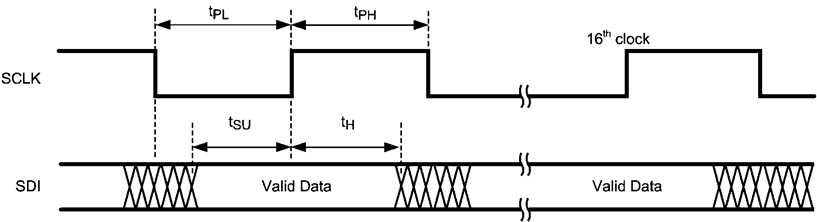 Figure 1. Write Timing Diagram
7.7 Read Timing Requirements
Unless otherwise noted, all limits specified at TA = 25°C, 2.7 V ≤ VDD ≤ 5.5 V, 1.65 ≤ VDDIO ≤ MIN(3.6 V, VDD), VREF = 2.4 V, fOSC = 409.6-kHz and a 10-pF capacitive load in parallel with a 10-kΩ load on SDO.| MIN | NOM | MAX | UNIT | |||
|---|---|---|---|---|---|---|
| tODZ | SDO Driven-to-Tristate Time | Measured at 10% / 90% point | 15 | ns | ||
| tOZD | SDO Tristate-to-Driven Time | Measured at 10% / 90% point | 15 | ns | ||
| tOD | SDO Output Delay Time | 10 | ns | |||
| tCSS | CSB Set-up Time | 5 | ns | |||
| tCSH | CSB Hold Time | 5 | ns | |||
| tIAG | Inter-Access Gap | 10 | ns | |||
| tDRDYB | Data Ready Bar at every 1/ODR second, see Figure 25 | 4/fOSC | s | |||
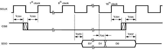 Figure 2. Read Timing Diagram
7.8 Typical Characteristics
All plots at TA = 25°C, VDD = 3.3 V, VDDIO = 1.8 V, VSS = VSSIO = 0 V, internal VREF = 2.4 V, VCM = RLDREF, internal fOSC = 409.6 kHz, data rate = 1067 sps, and High-Resolution mode, unless otherwise noted.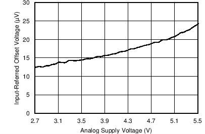 Figure 3. VOS vs VDD
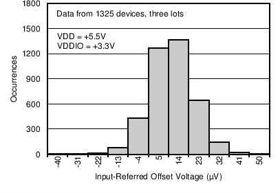 Figure 5. VOS Distribution
 Figure 7. Ibias vs VIN Diff
 Figure 9. Ibias vs VCM
 Figure 11. PSRR vs Frequency
 Figure 13. Input-Referred Noise
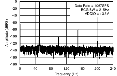 Figure 15. FFT Plot ECG Channel (50-Hz Signal)
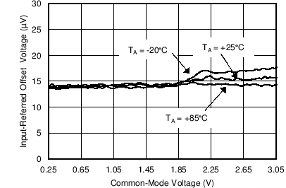 Figure 4. VOS vs VCM
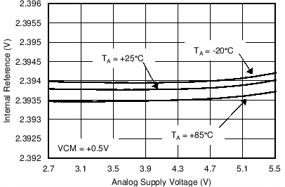 Figure 6. Vref vs VDD
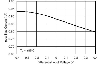 Figure 8. Ibias vs VIN Diff
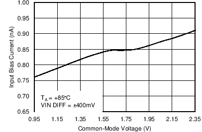 Figure 10. Ibias vs VCM
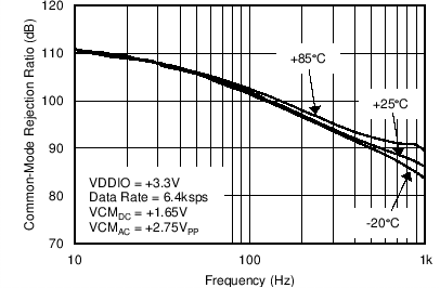 Figure 12. CMRR vs Frequency
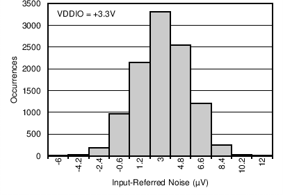 Figure 14. Noise Histogram
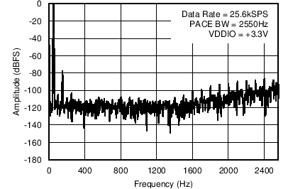 Figure 16. FFT Plot Pace Channel (50-Hz Signal)