SBAS561C June 2012 – January 2017 ADS131E04 , ADS131E06 , ADS131E08
PRODUCTION DATA.
- 1 Features
- 2 Applications
- 3 Description
- 4 Revision History
- 5 Device Comparison
- 6 Pin Configuration and Functions
- 7 Specifications
- 8 Parameter Measurement Information
-
9 Detailed Description
- 9.1 Overview
- 9.2 Functional Block Diagram
- 9.3 Feature Description
- 9.4 Device Functional Modes
- 9.5
Programming
- 9.5.1 Data Format
- 9.5.2 SPI Interface
- 9.5.3
SPI Command Definitions
- 9.5.3.1 Sending Multibyte Commands
- 9.5.3.2 WAKEUP: Exit STANDBY Mode
- 9.5.3.3 STANDBY: Enter STANDBY Mode
- 9.5.3.4 RESET: Reset Registers to Default Values
- 9.5.3.5 START: Start Conversions
- 9.5.3.6 STOP: Stop Conversions
- 9.5.3.7 OFFSETCAL: Channel Offset Calibration
- 9.5.3.8 RDATAC: Start Read Data Continuous Mode
- 9.5.3.9 SDATAC: Stop Read Data Continuous Mode
- 9.5.3.10 RDATA: Read Data
- 9.5.3.11 RREG: Read from Register
- 9.5.3.12 WREG: Write to Register
- 9.6
Register Map
- 9.6.1
Register Descriptions
- 9.6.1.1 ID: ID Control Register (Factory-Programmed, Read-Only) (address = 00h) [reset = xxh]
- 9.6.1.2 CONFIG1: Configuration Register 1 (address = 01h) [reset = 91h]
- 9.6.1.3 CONFIG2: Configuration Register 2 (address = 02h) [reset = E0h]
- 9.6.1.4 CONFIG3: Configuration Register 3 (address = 03h) [reset = 40]
- 9.6.1.5 FAULT: Fault Detect Control Register (address = 04h) [reset = 00h]
- 9.6.1.6 CHnSET: Individual Channel Settings (address = 05h to 0Ch) [reset = 10h]
- 9.6.1.7 FAULT_STATP: Fault Detect Positive Input Status (address = 12h) [reset = 00h]
- 9.6.1.8 FAULT_STATN: Fault Detect Negative Input Status (address = 13h) [reset = 00h]
- 9.6.1.9 GPIO: General-Purpose IO Register (address = 14h) [reset = 0Fh]
- 9.6.1
Register Descriptions
- 10Application and Implementation
- 11Power Supply Recommendations
- 12Layout
- 13Device and Documentation Support
- 14Mechanical, Packaging, and Orderable Information
Package Options
Mechanical Data (Package|Pins)
- PAG|64
Thermal pad, mechanical data (Package|Pins)
- PAG|64
Orderable Information
10 Application and Implementation
NOTE
Information in the following applications sections is not part of the TI component specification, and TI does not warrant its accuracy or completeness. TI’s customers are responsible for determining suitability of components for their purposes. Customers should validate and test their design implementation to confirm system functionality.
10.1 Application Information
10.1.1 Unused Inputs and Outputs
Power down unused analog inputs and connect them directly to AVDD.
Power down the Bias amplifier if unused and float OPAMPOUT and OPAMPN. Tie OPAMPP directly to AVSS or leave floating if unused.
Tie TESTN and TESTP to AVDD through individual 10-kΩ resistors or leave them floating if unused and the internal test signal is not used. If the internal test signal is used, leave TESTP and TESTN floating. If an external test signal is used, connect to external test circuitry.
Do not float unused digital inputs because excessive power-supply leakage current might result. Set the two-state mode setting pins high to DVDD or low to DGND through ≥10-kΩ resistors.
Pull DRDY to supply using weak pull-up resistor if unused.
If not daisy-chaining devices, tie DAISYIN directly to DGND.
10.1.2 Setting the Device Up for Basic Data Capture
This section outlines the procedure to configure the device in a basic state and capture data. This procedure is intended to put the device in a data sheet condition to check if the device is working properly in the user system. It is recommended that this procedure be followed initially to get familiar with the device settings. When this procedure is verified, the device can be configured as needed. For details on the timings for commands refer to the appropriate sections in the data sheet. The flow chart of Figure 53 details the initial ADS131E0x configuration and setup.
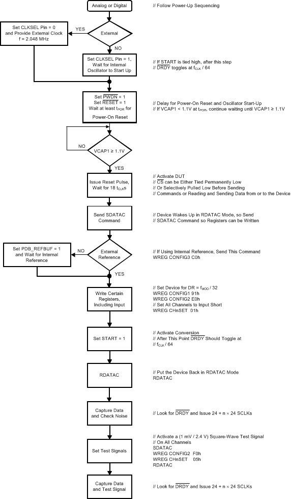 Figure 53. Initial Flow at Power Up
10.1.3 Multiple Device Configuration
The ADS131E0x provides configuration flexibility when multiple devices are used in a system. The serial interface typically needs four signals: DIN, DOUT, SCLK, and CS. With one additional chip select signal per device, multiple devices can be operated on the same SPI bus. The number of signals needed to interface to N devices is 3 + N.
10.1.3.1 Synchronizing Multiple Devices
When using multiple devices, the devices can be synchronized using the START signal. The delay time from the rising edge of the START signal to the falling edge of the DRDY signal is fixed for a given data rate (see the Start section for more details on the settling times). Figure 54 shows the behavior of two devices when synchronized with the START signal.
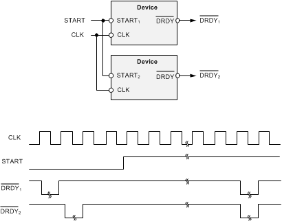 Figure 54. Synchronizing Multiple Converters
To use the internal oscillator in a daisy-chain configuration, one device must be set as the master for the clock source with the internal oscillator enabled (CLKSEL pin = 1) and the internal oscillator clock must be brought out of the device by setting the CLK_EN register bit to 1. The master device clock is used as the external clock source for the other devices.
There are two ways to connect multiple devices with an optimal number of interface pins: standard configuration and daisy-chain configuration.
10.1.3.2 Standard Configuration
Figure 55a shows a configuration with two ADS131E0x devices cascaded. Together, the devices create a system with up to 16 channels. DOUT, SCLK, and DIN are shared. Each device has its own chip select. When a device is not selected by the corresponding CS being driven to logic 1, the DOUT pin of this device is high-impedance. This structure allows the other device to take control of the DOUT bus. This configuration method is suitable for the majority of applications where extra I/O pins are available.
10.1.3.3 Daisy-Chain Configuration
Daisy-chain mode is enabled by setting the DAISY_IN bit in the CONFIG1 register. Figure 55b shows the daisy-chain configuration. In this mode SCLK, DIN, and CS are shared across multiple devices. The DOUT pin of device 1 is connected to the DAISY_IN pin of device 0, thereby creating a daisy-chain for the data. Connect the DAISY_IN pin of device 1 to DGND if not used. The daisy-chain timing requirements for the SPI interface are illustrated in Figure 2. Data from the ADS131E0x device 0 appear first on DOUT, followed by a don’t care bit, and then the status and data words from the ADS131E0x device 1.
The internal oscillator output cannot be enabled because all devices in the chain operate by sharing the same DIN pin, thus an external clock must be used.
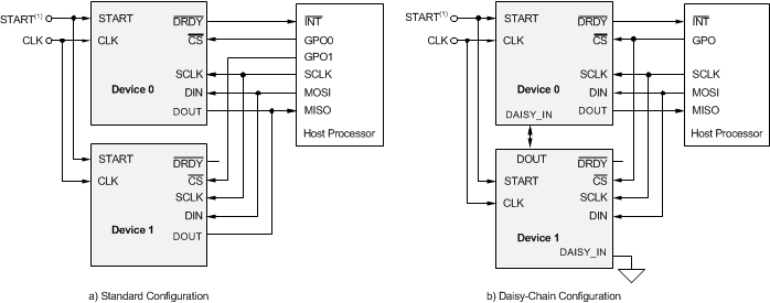
There are several items to be aware of when using daisy-chain mode:
- One extra SCLK must be issued between each data set (see Figure 56)
- All devices are configured to the same register values because the CS signal is shared
- Device register readback is only valid for device 0 in the daisy-chain. Only ADC conversion data can be read back from device 1 through device N, where N is the last device in the chain.
The more devices in the chain, the more challenging adhering to setup and hold times becomes. A star-pattern connection of SCLK to all devices, minimizing the trace length of DOUT, and other printed circuit board (PCB) layout techniques helps to mitigate this challenge with signal delays. Placing delay circuits (such as buffers) between DOUT and DAISY_IN are options to help reduce signal delays. One other option is to insert a D flip-flop between DOUT and DAISY_IN clocked on an inverted SCLK. Figure 56 shows a timing diagram for daisy-chain mode.

NOTE:
n = (number of channels) × (resolution) + 24 bits. The number of channels is 8. Resolution is 16 bits or 24 bits.The maximum number of devices that can be daisy-chained depends on the data rate that the devices are operated at. The maximum number of devices can be calculated with Equation 10.

where
- NBITS = device resolution (depends on DR[2:0] setting)
- NCHANNELS = number of channels powered up in the device
For example, when the ADS131E0x is operated in 24-bit, 8-kSPS data rate with fSCLK = 10 MHz, up to six devices can be daisy-chained together.
10.1.4 Power Monitoring Specific Applications
All channels of the ADS131E0x are exactly identical, yet independently configurable, thus giving the user the flexibility of selecting any channel for voltage or current monitoring. An overview of a system configured to monitor voltage and current is illustrated in Figure 57. Also, the simultaneously sampling capability of the device allows the user to monitor both the current and the voltage at the same time. The full-scale differential input voltage of each channel is determined by the PGA gain setting (see the CHnSET: Individual Channel Settings section) for the respective channel and VREF (see the CONFIG3: Configuration Register 3 section).
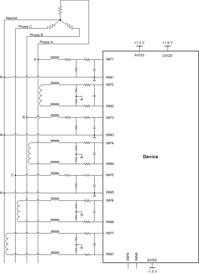 Figure 57. Overview of a Power-Monitoring System
10.1.5 Current Sensing
Figure 58 illustrates a simplified diagram of typical configurations used for current sensing with a Rogowski coil, current transformer (CT), or an air coil that outputs a current or voltage. In the case of a current output transformer, the burden resistors (R1) are used for current-to-voltage conversion. The output of the burden resistors is connected to the ADS131E0x INxP and INxN inputs through an antialiasing RC filter for current sensing. In the case of a voltage output transformer for current sensing (such as certain types of Rogowski coils), the output terminals of the transformer are directly connected to the ADS131E0x INxP and INxN inputs through an antialiasing RC filter. The input network must be biased to mid-supply if using a unipolar-supply analog configuration (AVSS = 0 V, AVDD = 2.7 V to 5.5 V). The common-mode bias voltage [(AVDD + AVSS) / 2] can be obtained from the ADS131E0x by either configuring the internal op amp in a unity-gain configuration using the RF resistor and setting the OPAMP_REF bit of the CONFIG3 register to 1, or generated externally with a resistor divider network between the positive and negative supplies.
Select the value of resistor R1 for the current output transformer and turns ratio of the transformer such that the ADS131E0x full-scale differential input voltage range is not exceeded. Likewise, select the output voltage for the voltage output transformer to not exceed the full-scale differential input voltage range. In addition, the selection of the resistors (R1 and R2) and turns ratio must not saturate the transformer over the full operating dynamic range. Figure 58a illustrates differential input current sensing and Figure 58b illustrates single-ended input voltage sensing. Use separate external op amps to source and sink current because the internal op amp has very limited current sink and source capability. Additionally, separate op amps for each channel help isolate individual phases from one another to limit crosstalk.
10.1.6 Voltage Sensing
Figure 59 illustrates a simplified diagram of commonly-used differential and single-ended methods of voltage sensing. A resistor divider network is used to step down the line voltage to within the acceptable ADS131E0x input range and then connect to the inputs (INxP and INxN) through an antialiasing RC filter formed by resistor R3 and capacitor C. The common-mode bias voltage [(AVDD + AVSS) / 2] can be obtained from the ADS131E0x by either configuring the internal op amp in a unity-gain configuration using the RF resistor and setting the OPAMP_REF bit of the CONFIG3 register, or generated externally by using a resistor divider network between the positive and negative supplies.
In either of the cases illustrated in Figure 59 (Figure 59a for a differential input and Figure 59b for a single-ended input), the line voltage is divided down by a factor of [R2 / (R1 + R2)]. Values of R1 and R2 must be carefully chosen so that the voltage across the ADS131E0x inputs (INxP and INxN) does not exceed the range of the ADS131E0x over the full operating dynamic range. Use separate external op amps to source and sink current because the internal op amp has very limited current sink and source capability. Additionally, separate op amps for each channel help isolate individual phases from one another to limit crosstalk.
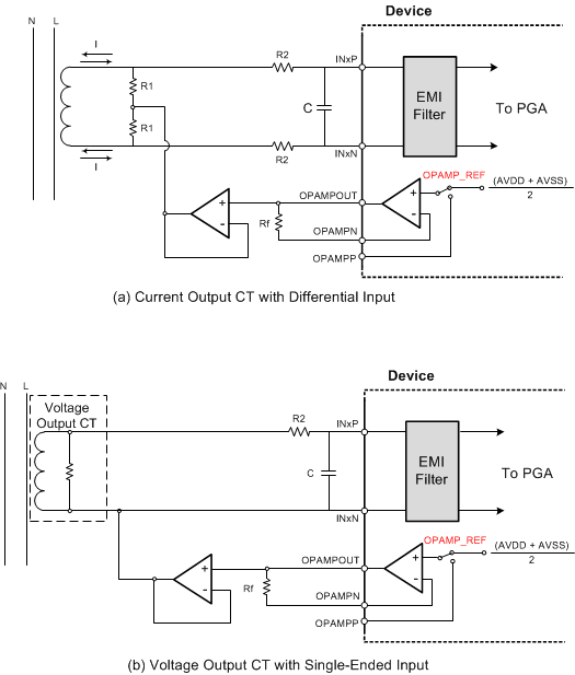 Figure 58. Simplified Current-Sensing Connections
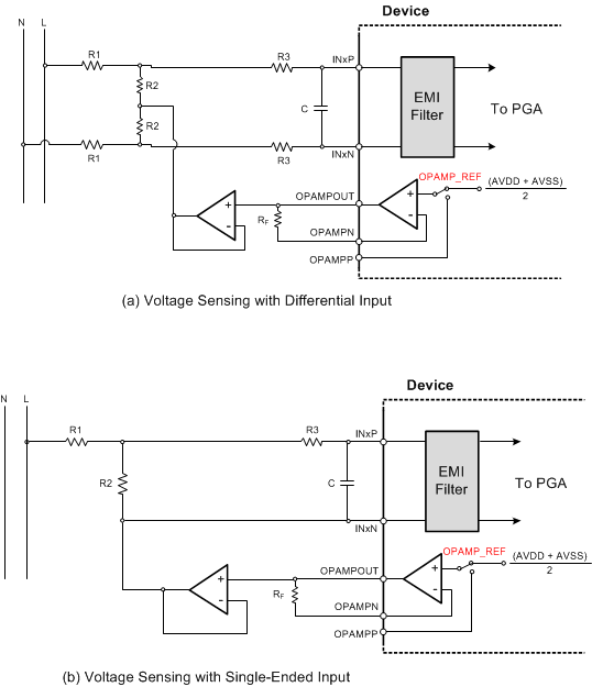 Figure 59. Simplified Voltage-Sensing Connections
10.2 Typical Application
Figure 60 shows the ADS131E0x being used as part of an electronic trip unit (ETU) in a circuit breaker or protection relay. Delta-sigma (ΔΣ), analog-to-digital converters (ADCs), such as the ADS131E0x, are ideal for this application because these devices provide a wide dynamic range.
The system measures voltages and currents output from a breaker enclosure. In this example, the first three inputs measure line voltage and the remaining five inputs measure line current from the secondary winding of a current transformer (CT). A voltage divider steps down the voltage from the output of the breaker. Several resistors are used to break up power consumption and are used as a form of fault protection against any potential resistor short-circuit. After the voltage step down, RC filters are used for antialiasing and diodes protect the inputs from overrange.
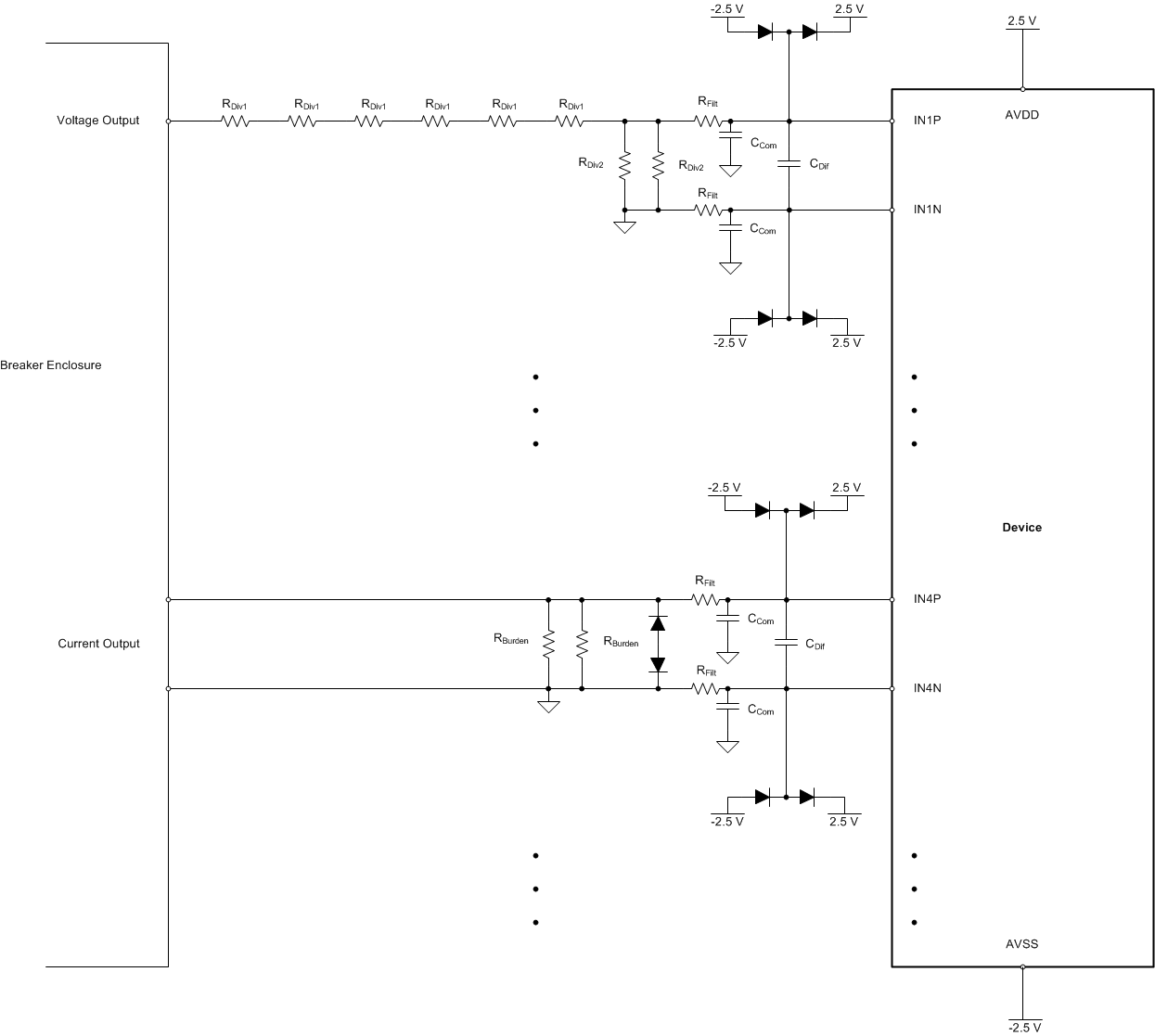 Figure 60. ETU Block Diagram: High-Resolution and Fast Power-Up Analog Front-End for Air Circuit Breaker or Molded Case Circuit Breaker and Protection Relay
10.2.1 Design Requirements
Table 21 summarizes the design requirements for the circuit breaker front-end application.
Table 21. ETU Circuit Breaker Design Requirements
| DESIGN PARAMETER | VALUE |
|---|---|
| Number of voltage inputs | 3 |
| Voltage input range | 10 V to 750 V |
| Number of current inputs | 5 |
| Current input range | 50 mA to 25 A |
| Dynamic range with fixed gain | > 500:1 |
| Accuracy | ±1% |
10.2.2 Detailed Design Procedure
The line voltage is stepped down to a voltage range within the measurable range of the ADC. The reference voltage determines the range in which the ADC can measure signals. The ADS131E0x has two integrated low-drift reference voltage options: 2.4 V and 4 V.
Equation 11 describes the transfer function for the voltage divider at the input in Figure 60. Using multiple series resistors, RDIV1, and multiple parallel resistors, RDIV2, allows for power and heat to be dissipated among several circuit elements and serves as protection against a potential short-circuit across a single resistor. The number of resistors trade off with nominal accuracy because each additional element introduces an additional source of tolerance.

The step-down resistor, RDiv2, dominates the measurement error produced by the resistor network. Using input PGAs on the ADS131E0x helps to mitigate this error source by allowing RDiv2 to be made smaller and then amplifying the signal to near full-scale using the ADS131E0x PGA.
For this design, RDiv1 is set to 200 kΩ and RDiv2 is set to 2.4 kΩ to provide proper signal attenuation at a sufficient power level across each resistor. The input saturates at values greater than ±750 V when using the ADS131E0x internal 2.4-V reference and a PGA gain of 2.
The ADS131E0x measures the line current by creating a voltage across the burden resistance (RBurden in Figure 60) in parallel with the secondary winding of a CT. As with the voltage measurement front-end, multiple resistors (RDiv1) that are used to step down a voltage share the duty of dissipating power. In this design, RBURDEN is set to 33 Ω. Used with a 1:500 turns ratio CT, the ADC input saturates with a line current over 25 A when the ADC is configured using the internal 2.4-V reference and a PGA gain of 2.
Diodes protect the ADS131E0x inputs from overvoltage and current. Diodes on each input shunt to either supply if the input voltage exceeds the safe range for the device. On current inputs, a diode shunts the inputs if current on the secondary winding of the CT threatens to damage the device.
The combination of RFilt, CCom, and CDif form the antialiasing filters for each of the inputs. The differential capacitor CDif improves the common-mode rejection of the system by sharing its tolerance between the positive and negative input. The antialiasing filter requirement is not strict because the nature of a ΔΣ converter (with oversampling and digital filter) attenuates a significant proportion of out-of-band noise. In addition, the input PGAs have intentionally low bandwidth to provide additional antialiasing. The component values used in this design are RFilt = 1 kΩ, CCom = 47 pF, and CDif = 0.015 μF. This first-order filter produces a relatively flat frequency response beyond 2 kHz, capable of measuring greater than 30 harmonics at a 50-Hz or 60-Hz fundamental frequency. The 3-dB cutoff frequency of the filter is 5.3 kHz for each input channel.
Each analog system block introduces errors from input to output. Protection CTs in the 5P accuracy class can introduce as much as ±1% current error from input to output. CTs in the 10P accuracy class can introduce as much as ±3% error. The burden resistor also introduces errors in the form of resistor tolerance and temperature drift. For the voltage input, error comes from the divider network in the form of resistor tolerance and temperature drift. Finally, the converter introduces errors in the form of offset error, gain error, and reference error. All of these specifications can drift over temperature.
10.2.3 Application Curves
Accuracy is measured using a system designed in a similar way to that illustrated in Figure 60. The CT used for the current input is CT1231 (a 0.3 class, solid core, 5:2500 turns transformer). In each case, data are taken for three channels over one cycle of the measured waveform and the RMS input-referred signal is compared to the output to calculate the error. The equation used to derive the measurement error is shown in Equation 12. Data are taken using both the 2.4-V and 4-V internal reference voltages. In all cases, measured accuracy is within ±1%.

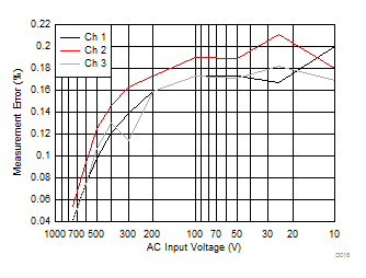
| One 50-Hz line cycle , 4-kSPS data rate, 80 samples, gain = 2, VREF = 2.4 V, measurement accuracy is absolute value |
2.4-V Reference
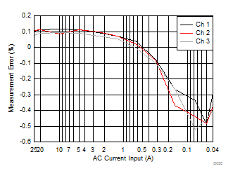
| One 50-Hz line cycle , 4-kSPS data rate, 80 samples, gain = 2, VREF = 2.4 V |
2.4-V Reference
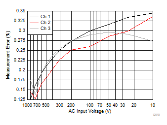
| One 50-Hz line cycle , 4-kSPS data rate, 80 samples, gain = 2, VREF = 4 V, measurement accuracy is absolute value |
4-V Reference
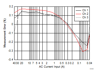
| One 50-Hz line cycle , 4-kSPS data rate, 80 samples, gain = 2, VREF = 4 V |
4-V Reference
 |
For a step-by-step design procedure, circuit schematics, bill of materials, PCB files, simulation results, and test results, see High Resolution, Fast Startup Analog Front End for Air Circuit Breaker Design Guide (TIDUB80). |