SLAS900F October 2012 – December 2014 ADS42JB49 , ADS42JB69
PRODUCTION DATA.
- 1 Features
- 2 Applications
- 3 Description
- 4 Revision History
- 5 Device Comparison Table
- 6 Pin Configuration and Functions
-
7 Specifications
- 7.1 Absolute Maximum Ratings
- 7.2 ESD Ratings
- 7.3 Recommended Operating Conditions
- 7.4 Thermal Information
- 7.5 Electrical Characteristics: ADS42JB69 (16-Bit)
- 7.6 Electrical Characteristics: ADS42JB49 (14-Bit)
- 7.7 Electrical Characteristics: General
- 7.8 Digital Characteristics
- 7.9 Timing Characteristics
- 7.10 Typical Characteristics: ADS42JB69
- 7.11 Typical Characteristics: ADS42JB49
- 7.12 Typical Characteristics: Common
- 7.13 Typical Characteristics: Contour
- 8 Parameter Measurement Information
-
9 Detailed Description
- 9.1 Overview
- 9.2 Functional Block Diagram
- 9.3 Feature Description
- 9.4 Device Functional Modes
- 9.5 Programming
- 9.6
Register Maps
- 9.6.1
Description of Serial Interface Registers
- 9.6.1.1 Register 6 (offset = 06h) [reset = 00h]
- 9.6.1.2 Register 7 (offset = 07h) [reset = 00h]
- 9.6.1.3 Register 8 (offset = 08h) [reset = 00h]
- 9.6.1.4 Register B (offset = 0Bh) [reset = 00h]
- 9.6.1.5 Register C (offset = 0Ch) [reset = 00h]
- 9.6.1.6 Register D (offset = 0Dh) [reset = 00h]
- 9.6.1.7 Register E (offset = 0Eh) [reset = 00h]
- 9.6.1.8 Register F (offset = 0Fh) [reset = 00h]
- 9.6.1.9 Register 10 (offset = 10h) [reset = 00h]
- 9.6.1.10 Register 11 (offset = 11h) [reset = 00h]
- 9.6.1.11 Register 12 (offset = 12h) [reset = 00h]
- 9.6.1.12 Register 13 (offset = 13h) [reset = 00h]
- 9.6.1.13 Register 1F (offset = 1Fh) [reset = FFh]
- 9.6.1.14 Register 26 (offset = 26h) [reset = 00h]
- 9.6.1.15 Register 27 (offset = 27h) [reset = 00h]
- 9.6.1.16 Register 2B (offset = 2Bh) [reset = 00h]
- 9.6.1.17 Register 2C (offset = 2Ch) [reset = 00h]
- 9.6.1.18 Register 2D (offset = 2Dh) [reset = 00h]
- 9.6.1.19 Register 30 (offset = 30h) [reset = 40h]
- 9.6.1.20 Register 36 (offset = 36h) [reset = 00h]
- 9.6.1.21 Register 37 (offset = 37h) [reset = 00h]
- 9.6.1.22 Register 38 (offset = 38h) [reset = 00h]
- 9.6.1
Description of Serial Interface Registers
- 10Application and Implementation
- 11Power Supply Recommendations
- 12Layout
- 13Device and Documentation Support
- 14Mechanical, Packaging, and Orderable Information
Package Options
Mechanical Data (Package|Pins)
- RGC|64
Thermal pad, mechanical data (Package|Pins)
- RGC|64
Orderable Information
10 Application and Implementation
NOTE
Information in the following applications sections is not part of the TI component specification, and TI does not warrant its accuracy or completeness. TI’s customers are responsible for determining suitability of components for their purposes. Customers should validate and test their design implementation to confirm system functionality.
10.1 Application Information
In a typical application (such as a dual-channel digitizer) the ADS42JBx9 is connected to a field-programmable gate array (FPGA) or application-specific integrated circuit (ASIC), as shown in Figure 110. A device clock and SYSREF signal must be provided to the ADC. TI recommends that the device clock and SYSREF are source synchronous (generated from a common source with matched trace lengths) if synchronizing multiple ADCs. An example of a device that can be used to generate a source-synchronous device clock and SYSREF is the LMK04828. The device clock frequency must be the same frequency as the desired sampling rate. The SYSREF period is required to be an integer multiple of the period of the multi-frame clock. Consequently, the frequency of SYSREF must be restricted to Equation 1
where
- n = 1, 2, 3 and so forth,
- 1< K < 32 (set by SPI register address 2Dh), and
- F = 1, (two lanes per ADC mode), F = 2 (one lane per ADC mode).
A large enough K is recommended (greater than 16) to absorb the lane skews and avoid data transmission errors across the JESD204B interface. The SYNC~ signal is used by the FPGA or ASIC to acknowledge the correction reception of comma characters from the ADC during the JESD204B link initialization process. During normal operation this signal must be logic 1 if there are no errors in the data transmission from the ADC to the FPGA or ASIC.
10.2 Typical Application
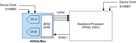 Figure 110. The ADS42JBx9 in a Dual-Channel Digitizer
10.2.1 Design Requirements
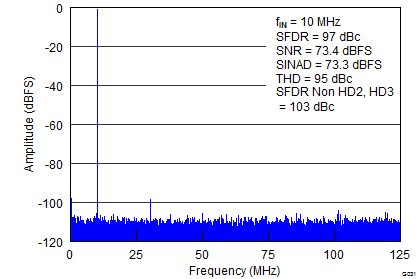
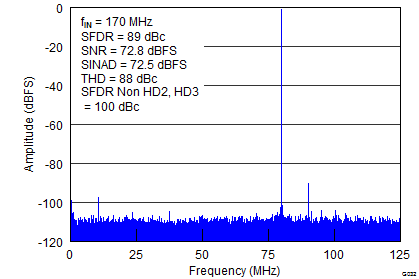
For this design example, use the parameters listed in Table 39 as the input parameters.
Table 39. Design Parameters
| DESIGN PARAMETER | EXAMPLE VALUE |
|---|---|
| fSAMPLE | 245.76 MSPS |
| Input frequency (IF) | 10 MHz (Figure 122), 170 MHz (Figure 123) |
| Signal-to-noise ratio (SNR) | > 72 dBc |
| Spurious-free dynamic range (SFDR) | > 80 dBc |
| Second-order harmonic distortion (HD2) | > 90 dBc |
10.2.2 Detailed Design Procedure
10.2.2.1 Analog Input
The analog input pins have analog buffers (running from the AVDD3V supply) that internally drive the differential sampling circuit. As a result of the analog buffer, the input pins present high input impedance to the external driving source (10-kΩ dc resistance and 4-pF input capacitance). The buffer helps isolate the external driving source from the switching currents of the sampling circuit. This buffering makes driving the buffered inputs easier than when compared to an ADC without the buffer.
The input common-mode is set internally using a 5-kΩ resistor from each input pin to VCM so the input signal can be ac-coupled to the pins. Each input pin (INP, INM) must swing symmetrically between VCM + 0.5 V and VCM – 0.5 V, resulting in a 2-V PP differential input swing. When programmed for 2.5-V PP full-scale, each input pin must swing symmetrically between VCM + 0.625 V and VCM – 0.625 V.
The input sampling circuit has a high 3-dB bandwidth that extends up to 900 MHz (measured with a 50-Ω source driving a 50-Ω termination between INP and INM). The dynamic offset of the first-stage sub-ADC limits the maximum analog input frequency to approximately 250 MHz (with a 2.5-VPP full-scale amplitude) and to approximately 400 MHz (with a 2-VPP full-scale amplitude). This 3-dB bandwidth is different than the analog bandwidth of 900 MHz, which is only an indicator of signal amplitude versus frequency.
10.2.2.1.1 Drive Circuit Requirements
For optimum performance, the analog inputs must be driven differentially. This technique improves the common-mode noise immunity and even-order harmonic rejection. A small resistor (5 Ω to 10 Ω) in series with each input pin is recommended to damp out ringing caused by package parasitics.
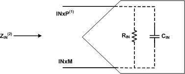
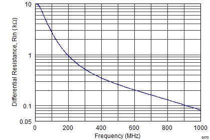
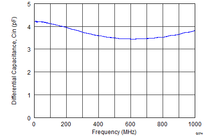
Figure 111, Figure 112, and Figure 113 illustrate the differential impedance (ZIN = RIN || CIN) at the ADC input pins. The presence of the analog input buffer results in an almost constant input capacitance up to 1 GHz.
10.2.2.1.2 Driving Circuit
An example driving circuit configuration is shown in Figure 114. To optimize even-harmonic performance at high input frequencies (greater than the first Nyquist), the use of back-to-back transformers is recommended, as shown in Figure 114. Note that the drive circuit is terminated by 50 Ω near the ADC side. The ac-coupling capacitors allow the analog inputs to self-bias around the required common-mode voltage. An additional R-C-R (39 Ω - 6.8 pF - 39 Ω) circuit placed near device pins helps further improve HD3.
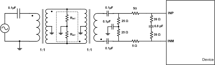 Figure 114. Drive Circuit for Input Frequencies up to 250 MHz
The mismatch in the transformer parasitic capacitance (between the windings) results in degraded even-order harmonic performance. Connecting two identical RF transformers back-to-back helps minimize this mismatch and good performance is obtained for high-frequency input signals. An additional termination resistor pair may be required between the two transformers, as shown in Figure 114. The center point of this termination is connected to ground to improve the balance between the P (positive) and M (negative) sides. The values of the terminations between the transformers and on the secondary side must be chosen to obtain an effective 50 Ω (for a 50-Ω source impedance). For high input frequencies (> 250 MHz), the R-C-R circuit can be removed as indicated in Figure 115.
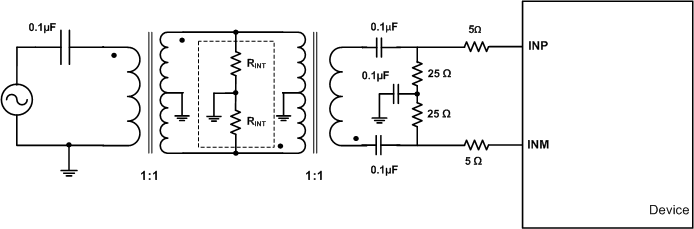 Figure 115. Drive Circuit for Input Frequencies > 250 MHz
10.2.2.2 Clock Input
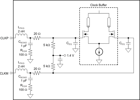
The device clock inputs can be driven differentially (sine, LVPECL, or LVDS) or single-ended (LVCMOS), with little or no difference in performance between them. The common-mode voltage of the clock inputs is set to 1.4 V using internal 5-kΩ resistors. The self-bias clock inputs of the ADS42JB69 and ADS42JB49 can be driven by the transformer-coupled, sine-wave clock source or by the ac-coupled, LVPECL and LVDS clock sources, as shown in Figure 116, Figure 117, and Figure 118. Figure 119 details the internal clock buffer.
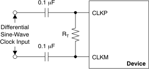
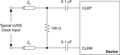 Figure 117. LVDS Clock Driving Circuit
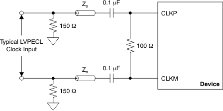 Figure 118. LVPECL Clock Driving Circuit
A single-ended CMOS clock can be ac-coupled to the CLKP input, with CLKM connected to ground with a 0.1-μF capacitor, as shown in Figure 120. However, for best performance the clock inputs must be driven differentially, thereby reducing susceptibility to common-mode noise. For high input frequency sampling, TI recommends using a clock source with very low jitter. Band-pass filtering of the clock source can help reduce the effects of jitter. There is no change in performance with a non-50% duty cycle clock input.
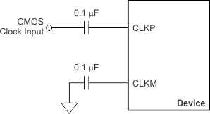 Figure 120. Single-Ended Clock Driving Circuit
10.2.2.2.1 SNR and Clock Jitter
The signal-to-noise ratio (SNR) of the ADC is limited by three different factors, as shown in Equation 2. Quantization noise is typically not noticeable in pipeline converters and is 96 dBFS for a 16-bit ADC. Thermal noise limits SNR at low input frequencies and clock jitter sets SNR for higher input frequencies.

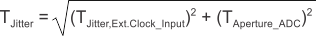
SNR limitation is a result of sample clock jitter and can be calculated by Equation 3:

The total clock jitter (TJitter) has three components: the internal aperture jitter (85 fS for the device) is set by the noise of the clock input buffer, the external clock jitter, and the jitter from the analog input signal. TJitter can be calculated by Equation 4:
External clock jitter can be minimized by using high-quality clock sources and jitter cleaners as well as band-pass filters at the clock input while a faster clock slew rate improves ADC aperture jitter. The device has a 74.1-dBFS thermal noise and an 85-fS internal aperture jitter. The SNR value depends on the amount of external jitter for different input frequencies, as shown in Figure 121.
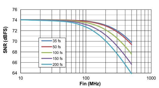 Figure 121. SNR versus Input Frequency and External Clock Jitter
10.2.3 Application Curves