SLAS900F October 2012 – December 2014 ADS42JB49 , ADS42JB69
PRODUCTION DATA.
- 1 Features
- 2 Applications
- 3 Description
- 4 Revision History
- 5 Device Comparison Table
- 6 Pin Configuration and Functions
-
7 Specifications
- 7.1 Absolute Maximum Ratings
- 7.2 ESD Ratings
- 7.3 Recommended Operating Conditions
- 7.4 Thermal Information
- 7.5 Electrical Characteristics: ADS42JB69 (16-Bit)
- 7.6 Electrical Characteristics: ADS42JB49 (14-Bit)
- 7.7 Electrical Characteristics: General
- 7.8 Digital Characteristics
- 7.9 Timing Characteristics
- 7.10 Typical Characteristics: ADS42JB69
- 7.11 Typical Characteristics: ADS42JB49
- 7.12 Typical Characteristics: Common
- 7.13 Typical Characteristics: Contour
- 8 Parameter Measurement Information
-
9 Detailed Description
- 9.1 Overview
- 9.2 Functional Block Diagram
- 9.3 Feature Description
- 9.4 Device Functional Modes
- 9.5 Programming
- 9.6
Register Maps
- 9.6.1
Description of Serial Interface Registers
- 9.6.1.1 Register 6 (offset = 06h) [reset = 00h]
- 9.6.1.2 Register 7 (offset = 07h) [reset = 00h]
- 9.6.1.3 Register 8 (offset = 08h) [reset = 00h]
- 9.6.1.4 Register B (offset = 0Bh) [reset = 00h]
- 9.6.1.5 Register C (offset = 0Ch) [reset = 00h]
- 9.6.1.6 Register D (offset = 0Dh) [reset = 00h]
- 9.6.1.7 Register E (offset = 0Eh) [reset = 00h]
- 9.6.1.8 Register F (offset = 0Fh) [reset = 00h]
- 9.6.1.9 Register 10 (offset = 10h) [reset = 00h]
- 9.6.1.10 Register 11 (offset = 11h) [reset = 00h]
- 9.6.1.11 Register 12 (offset = 12h) [reset = 00h]
- 9.6.1.12 Register 13 (offset = 13h) [reset = 00h]
- 9.6.1.13 Register 1F (offset = 1Fh) [reset = FFh]
- 9.6.1.14 Register 26 (offset = 26h) [reset = 00h]
- 9.6.1.15 Register 27 (offset = 27h) [reset = 00h]
- 9.6.1.16 Register 2B (offset = 2Bh) [reset = 00h]
- 9.6.1.17 Register 2C (offset = 2Ch) [reset = 00h]
- 9.6.1.18 Register 2D (offset = 2Dh) [reset = 00h]
- 9.6.1.19 Register 30 (offset = 30h) [reset = 40h]
- 9.6.1.20 Register 36 (offset = 36h) [reset = 00h]
- 9.6.1.21 Register 37 (offset = 37h) [reset = 00h]
- 9.6.1.22 Register 38 (offset = 38h) [reset = 00h]
- 9.6.1
Description of Serial Interface Registers
- 10Application and Implementation
- 11Power Supply Recommendations
- 12Layout
- 13Device and Documentation Support
- 14Mechanical, Packaging, and Orderable Information
Package Options
Mechanical Data (Package|Pins)
- RGC|64
Thermal pad, mechanical data (Package|Pins)
- RGC|64
Orderable Information
12 Layout
12.1 Layout Guidelines
- The length of the positive and negative traces of a differential pair must be matched to within 2 mils of each other.
- Each differential pair length must be matched within 10 mils of each other.
- When the ADC is used on the same printed circuit board (PCB) with a digital intensive component (such as an FPGA or ASIC), separate digital and analog ground planes must be used. Do not overlap these separate ground planes to minimize undesired coupling.
- Connect decoupling capacitors directly to ground and place these capacitors close to the ADC power pins and the power-supply pins to filter high-frequency current transients directly to the ground plane, as shown in Figure 125.
- Ground and power planes must be wide enough to keep the impedance very low. In a multilayer PCB, one layer each must be dedicated to ground and power planes.
- All high-speed SERDES traces must be routed straight with minimum bends. Where a bend is necessary, avoid making very sharp right angle bends in the trace.
- FR4 material can be used for the PCB core dielectric, up to the maximum 3.125 Gbps bit rate supported by the ADS42JBx9 device family. Path loss can be compensated for by adjusting the drive strength from the device using SPI register 36h.
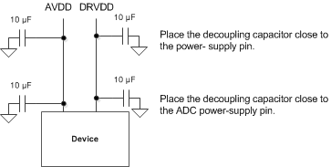 Figure 125. Recommended Placement of Power-Supply Decoupling Capacitors
12.2 Layout Example
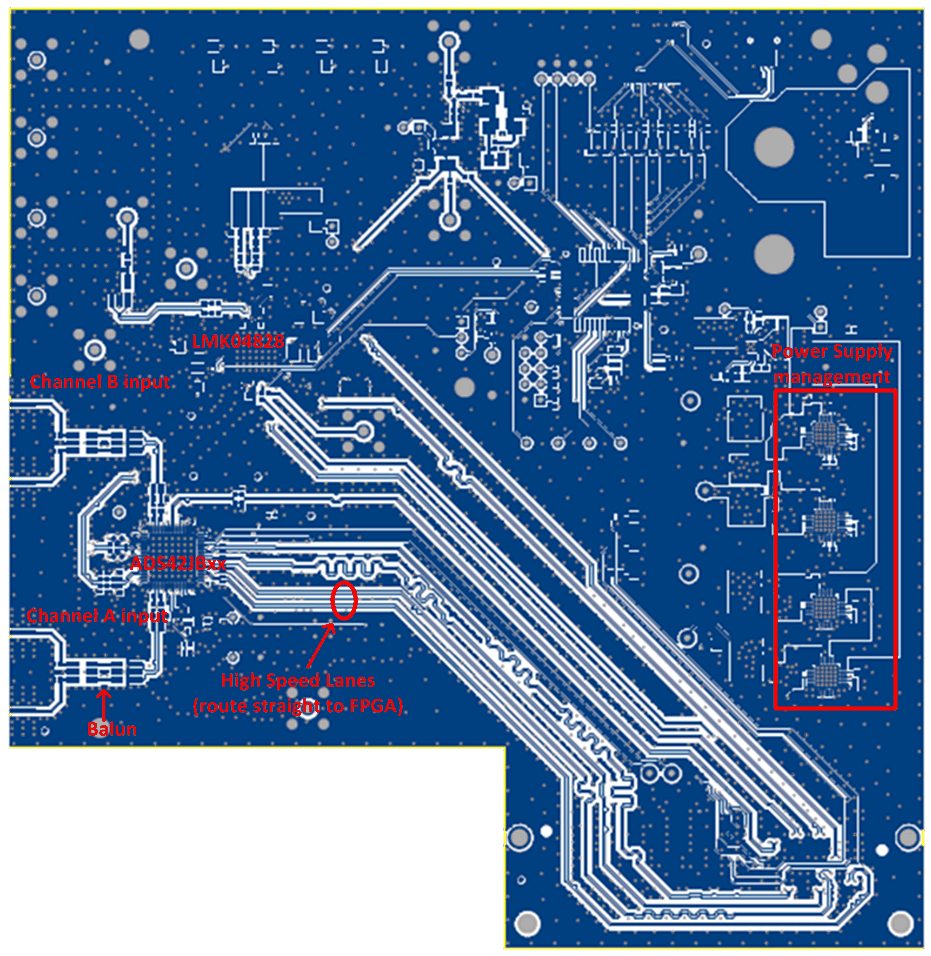 Figure 126. ADS42JBx9 EVM Top Layer