SLAS900F October 2012 – December 2014 ADS42JB49 , ADS42JB69
PRODUCTION DATA.
- 1 Features
- 2 Applications
- 3 Description
- 4 Revision History
- 5 Device Comparison Table
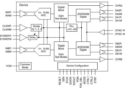
- 6 Pin Configuration and Functions
-
7 Specifications
- 7.1 Absolute Maximum Ratings
- 7.2 ESD Ratings
- 7.3 Recommended Operating Conditions
- 7.4 Thermal Information
- 7.5 Electrical Characteristics: ADS42JB69 (16-Bit)
- 7.6 Electrical Characteristics: ADS42JB49 (14-Bit)
- 7.7 Electrical Characteristics: General
- 7.8 Digital Characteristics
- 7.9 Timing Characteristics
- 7.10 Typical Characteristics: ADS42JB69
- 7.11 Typical Characteristics: ADS42JB49
- 7.12 Typical Characteristics: Common
- 7.13 Typical Characteristics: Contour
- 8 Parameter Measurement Information
-
9 Detailed Description
- 9.1 Overview
- 9.2 Functional Block Diagram
- 9.3 Feature Description
- 9.4 Device Functional Modes
- 9.5 Programming
- 9.6
Register Maps
- 9.6.1
Description of Serial Interface Registers
- 9.6.1.1 Register 6 (offset = 06h) [reset = 00h]
- 9.6.1.2 Register 7 (offset = 07h) [reset = 00h]
- 9.6.1.3 Register 8 (offset = 08h) [reset = 00h]
- 9.6.1.4 Register B (offset = 0Bh) [reset = 00h]
- 9.6.1.5 Register C (offset = 0Ch) [reset = 00h]
- 9.6.1.6 Register D (offset = 0Dh) [reset = 00h]
- 9.6.1.7 Register E (offset = 0Eh) [reset = 00h]
- 9.6.1.8 Register F (offset = 0Fh) [reset = 00h]
- 9.6.1.9 Register 10 (offset = 10h) [reset = 00h]
- 9.6.1.10 Register 11 (offset = 11h) [reset = 00h]
- 9.6.1.11 Register 12 (offset = 12h) [reset = 00h]
- 9.6.1.12 Register 13 (offset = 13h) [reset = 00h]
- 9.6.1.13 Register 1F (offset = 1Fh) [reset = FFh]
- 9.6.1.14 Register 26 (offset = 26h) [reset = 00h]
- 9.6.1.15 Register 27 (offset = 27h) [reset = 00h]
- 9.6.1.16 Register 2B (offset = 2Bh) [reset = 00h]
- 9.6.1.17 Register 2C (offset = 2Ch) [reset = 00h]
- 9.6.1.18 Register 2D (offset = 2Dh) [reset = 00h]
- 9.6.1.19 Register 30 (offset = 30h) [reset = 40h]
- 9.6.1.20 Register 36 (offset = 36h) [reset = 00h]
- 9.6.1.21 Register 37 (offset = 37h) [reset = 00h]
- 9.6.1.22 Register 38 (offset = 38h) [reset = 00h]
- 9.6.1
Description of Serial Interface Registers
- 10Application and Implementation
- 11Power Supply Recommendations
- 12Layout
- 13Device and Documentation Support
- 14Mechanical, Packaging, and Orderable Information
Package Options
Mechanical Data (Package|Pins)
- RGC|64
Thermal pad, mechanical data (Package|Pins)
- RGC|64
Orderable Information
9 Detailed Description
9.1 Overview
The ADS42JB69 and ADS42JB49 is a family of high linearity, buffered analog input, dual-channel ADCs with maximum sampling rates up to 250 MSPS employing JESD204B interface. The conversion process is initiated by a rising edge of the external input clock and the analog input signal is sampled. The sampled signal is sequentially converted by a series of small resolution stages, with the outputs combined in a digital correction logic block. At every clock edge the sample propagates through the pipeline, resulting in a data latency of 23 clock cycles. The output is available in CML logic levels following JESD204B standard.
9.2 Functional Block Diagram
9.3 Feature Description
9.3.1 Digital Gain
The device includes gain settings that can be used to obtain improved SFDR performance (compared to no gain). Gain is programmable from –2 dB to 6 dB (in 0.5-dB steps). For each gain setting, the analog input full-scale range scales proportionally. Table 2 shows how full-scale input voltage changes when digital gain are programmed in 1-dB steps. Refer to Table 19 to set digital gain using a serial interface register.
SFDR improvement is achieved at the expense of SNR; for 1 dB increase in digital gain, SNR degrades approximately between 0.5 dB and 1 dB. Therefore, gain can be used as a trade-off between SFDR and SNR. Note that the default gain after reset is 0 dB with a 2.0-VPP full-scale voltage.
Table 2. Full-Scale Range Across Gains
| DIGITAL GAIN | FULL-SCALE INPUT VOLTAGE |
|---|---|
| –2 dB | 2.5 VPP(1) |
| –1 dB | 2.2 VPP |
| 0 dB (default) | 2.0 VPP |
| 1 dB | 1.8 VPP |
| 2 dB | 1.6 VPP |
| 3 dB | 1.4 VPP |
| 4 dB | 1.25 VPP |
| 5 dB | 1.1 VPP |
| 6 dB | 1.0 VPP |
9.3.2 Input Clock Divider
The device is equipped with an internal divider on the clock input. This divider allows operation with a faster input clock, simplifying the system clock distribution design. The clock divider can be bypassed (divide-by-1) for operation with a 250-MHz clock. The divide-by-2 option supports a maximum 500-MHz input clock and the divide-by-4 option supports a maximum 1-GHz input clock frequency.
9.3.3 Overrange Indication
The device provides two different overrange indications. Normal OVR (default) is triggered if the final 16-bit data output exceeds the maximum code value. Fast OVR is triggered if the input voltage exceeds the programmable overrange threshold and is presented after only nine clock cycles, thus enabling a quicker reaction to an overrange event. By default, the normal overrange indication is output on the OVRA and OVRB pins. Using the register bit FAST OVR EN, the fast OVR indication can be presented on the overrange pins instead.
The input voltage level at which the overload is detected is referred to as the threshold and is programmable using the FAST OVR THRESHOLD bits. FAST OVR is triggered nine output clock cycles after the overload condition occurs. The threshold voltage amplitude at which fast OVR is triggered is:
1 × [the decimal value of the FAST OVR THRESH bits] / 127
When digital is programmed (for gain values > 0 dB), the threshold voltage amplitude is:
10–Gain / 20 × [the decimal value of the FAST OVR THRESH bits] / 127
9.3.4 Pin Controls
The device power-down functions can be controlled either through the parallel control pins (STBY, PDN_GBL, CTRL1, and CTRL2) or through an SPI register setting.
STBY places the device in a standby power-down mode. PDN_GBL places the device in global power-down mode.
Table 3. CTRL1, CTRL2 Pin Functions
| CTRL1 | CTRL2 | DESCRIPTION |
|---|---|---|
| Low | Low | Normal operation |
| High | Low | Channel A powered down |
| Low | High | Channel B powered down |
| High | High | Global power-down |
Table 4. PDN_GBL Pin Function
| PDN_GBL | DESCRIPTION |
|---|---|
| Low | Normal operation |
| High | Global power-down. Wake-up from this mode is slow. |
Table 5. STBY Pin Function
| STBY | DESCRIPTION |
|---|---|
| Low | Normal operation |
| High | ADCs are powered down while the input clock buffer and output CML buffers are alive. Wake-up from this mode is fast. |
9.4 Device Functional Modes
9.4.1 JESD204B Interface
The JESD interface of ADS42JB49 and ADS42JB69, as shown in Figure 78, supports device subclasses 0, 1, and 2 with a maximum output data rate (per lane) of 3.125 Gbps.
An external SYSREF (subclass 1) or SYNC~ (subclass 2) signal is used to align all internal clock phases and the local multiframe clock to a specific sampling clock edge. This alignment allows synchronization of multiple devices in a system and minimizes timing and alignment uncertainty.
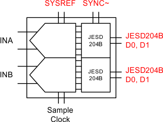 Figure 78. JESD204B Interface
Depending on the ADC sampling rate, the JESD204B output interface can be operated with either one or two lanes per ADC. The JESD204B interface can be configured using serial registers.
The JESD204B transmitter block (Figure 79) consists of the transport layer, the data scrambler, and the link layer. The transport layer maps the ADC output data into the selected JESD204B frame data format and manages if the ADC output data or test patterns are transmitted. The link layer performs the 8b and 10b data encoding as well as the synchronization and initial lane alignment using the SYNC~ input signal. Optionally, data from the transport layer can be scrambled.
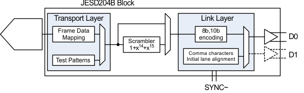 Figure 79. JESD204B Block
9.4.1.1 JESD204B Initial Lane Alignment (ILA)
When receiving device asserts the SYNC~ signal ( i.e a logic low signal is applied on SYNC~P - SYNC~M), the device begins transmitting comma (K28.5) characters to establish code group synchronization (CGS).
When synchronization is complete, the receiving device de-asserts the SYNC~ signal and the ADS42JB49 and ADS42JB69 begin the initial lane alignment (ILA) sequence with the next local multiframe clock boundary. The device transmits four multiframes, each containing K frames (where K is SPI programmable). Each multiframe contains the frame start and end symbols; the second multiframe also contains the JESD204 link configuration data.
9.4.1.2 JESD204B Test Patterns
There are three different test patterns available in the transport layer of the JESD204B interface. The device supports a clock output, an encoded, and a PRBS (215 – 1) pattern. These patterns can be enabled by serial register write in address 26h, bits D[7:6].
9.4.1.3 JESD204B Frame Assembly
The JESD204B standard defines the following parameters:
- L is the number of lanes per Lane.
- M is the number of converters per device.
- F is the number of octets per frame clock period.
- S is the number of samples per frame.
Table 6 lists the available JESD204B formats and valid device ranges. Ranges are limited by the maximum ADC sample frequency and the SERDES line rate.
Table 6. JESD240B Ranges
| L | M | F | S | MAX ADC SAMPLING RATE (MSPS) | MAX fSERDES (Gbps) |
|---|---|---|---|---|---|
| 4 | 2 | 1 | 1 | 250 | 2.5 |
| 2 | 2 | 2 | 1 | 156.25 | 3.125 |
The detailed frame assembly in 10x and 20x modes for dual-channel operation is shown in Table 7. Note that unused lanes in 10x mode become 3-stated.
Table 7. Frame Assembly for Dual-Channel Mode(1)
| LANE | LMF = 421 | LMF = 222 | ||||||||
|---|---|---|---|---|---|---|---|---|---|---|
| DA0 | A0[15:8] | A1[15:8] | A2[15:8] | A0[15:8] | A0[7:0] | A1[15:8] | A1[7:0] | A2[15:8] | A2[7:0] | |
| DA1 | A0[7:0] | A1[7:0] | A2[7:0] | — | — | — | — | — | — | |
| DB0 | B0[15:8] | B1[15:8] | B2[15:8] | B0[15:8] | B0[7:0] | B1[15:8] | B1[7:0] | B2[15:8] | B2[7:0] | |
| DB1 | B0[7:0] | B1[7:0] | B2[7:0] | — | — | — | — | — | — | |
9.4.1.4 JESD Link Configuration
During the lane alignment sequence, the ADS42JB69 and ADS42JB49 transmit JESD204B configuration parameters in the second multi-frame of the ILA sequence. Configuration bits are mapped in octets, as per the JESD204B standard described in Figure 80 and Table 8.
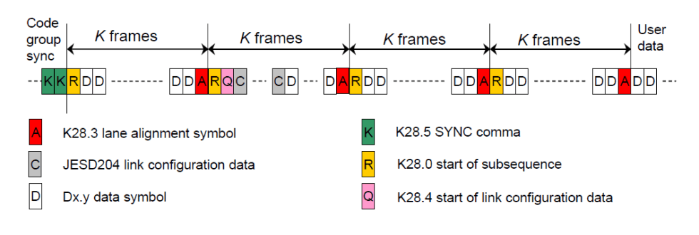 Figure 80. Initial Lane Alignment Sequence
Table 8. Mapping of Configuration Bits to Octets
| OCTET NO. | MSB | D6 | D5 | D4 | D3 | D2 | D1 | LSB |
|---|---|---|---|---|---|---|---|---|
| 0 | DID[7:0] | |||||||
| 1 | ADJCNT[3:0] | BID[3:0] | ||||||
| 2 | X | ADJDIR[0] | PHADJ[0] | LID[4:0] | ||||
| 3 | SCR[0] | L[4:0] | ||||||
| 4 | F[7:0] | |||||||
| 5 | K[4:0] | |||||||
| 6 | M[7:0] | |||||||
| 7 | CS[1:0] | X | N[4:0] | |||||
| 8 | SUBCLASSV[2:0] | N'[4:0] | ||||||
| 9 | JESDV[2:0] | S[4:0] | ||||||
| 10 | HD[0] | X | X | CF[4:0] | ||||
| 11 | RES1[7:0] | |||||||
| 12 | RES2[7:0] | |||||||
| 13 | FCHK[7:0] | |||||||
9.4.1.4.1 Configuration for 2-Lane (20x) SERDES Mode
Table 9 lists the values of the JESD204B configuration bits applicable for the 2-lane SERDES Mode. The default value of these bits after reset is also specified in the table.
Table 9. Configuration for 2-Lane SERDES Mode
| PARAMETER | DESCRIPTION | PARAMETER RANGE | FIELD | ENCODING | DEFAULT VALUE AFTER RESET |
|---|---|---|---|---|---|
| ADJCNT | Number of adjustment resolution steps to adjust DAC LMFC. Applies to subclass 2 operation only. | 0-15 | ADJCNT[3:0] | Binary value | 0 |
| ADJDIR | Direction to adjust DAC LMFC 0 : Advance 1 : Delay applies to subclass 2 operation only |
0-1 | ADJDIR[0] | Binary value | 0 |
| BID | Bank ID – extension to DID | 0-15 | BID[3:0] | Binary value | 0 |
| CF | No. of control words per frame clock period per link | 0-32 | CF[4:0] | Binary value | 0 |
| CS | No. of control bits per sample | 0-3 | CS[1:0] | Binary value | 0 |
| DID | Device (= link) identification no. | 0-255 | DID[7:0] | Binary value | 0 |
| F | No. of octets per frame | 1-256 | F[7:0] | Binary value minus 1 | 1 |
| HD | High-density format | 0-1 | HD[0] | Binary value | 0 |
| JESDV | JESD204 version 000 : JESD204A 001 : JESD204B |
0-7 | JESDV[2:0] | Binary value | 1 |
| K | No. of frames per multi-frame | 1-32 | K[4:0] | Binary value minus 1 | 8 |
| L | No. of lanes per converter device (link) | 1-32 | L[4:0] | Binary value minus 1 | 0 |
| LID | Lane identification no. (within link) | 0-31 | LID[4:0] | Binary value | LID[0] = 0, LID[1] = 1 |
| M | No. of converters per device | 1-256 | M[7:0] | Binary value minus 1 | 1 |
| N | Converter resolution | 1-32 | N[4:0] | Binary value minus 1 | 15 |
| N’ | Total no. of bits per sample | 1-32 | N'[4:0] | Binary value minus 1 | 15 |
| PHADJ | Phase adjustment request to DAC subclass 2 only. | 0-1 | PHADJ[0] | Binary value | 0 |
| S | No. of samples per converter per frame cycle | 1-32 | S[4:0] | Binary value minus 1 | 0 |
| SCR | Scrambling enabled | 0-1 | SCR[0] | Binary value | 0 |
| SUBCLASSV | Device subclass version 000 : Subclass 0 001 : Subclass 1 010 : Subclass 2 |
0-7 | SUBCLASSV[2:0] | Binary value | 2 |
| RES1 | Device subclass version 000 : Subclass 0 001 : Subclass 1 010 : Subclass 2 |
0-255 | RES1[7:0] | Binary value | 0 |
| RES2 | Reserved field 2 | 0-255 | RES2[7:0] | Binary value | 0 |
| CHKSUM | Checksum Σ (all above fields) mod 256 | 0-255 | FCHK[7:0] | Binary value | 44, 45 |
9.4.1.4.2 Configuration for 4-Lane (10x) SERDES Mode
Table 10 lists the values of the JESD204 configuration bits applicable for the 4-lane SERDES Mode. The default value of these bits after reset is also specified in the table.
Table 10. Configuration for 4-Lane SERDES Mode
| PARAMETER | DESCRIPTION | PARAMETER RANGE | FIELD | ENCODING | DEFAULT VALUE AFTER RESET |
|---|---|---|---|---|---|
| ADJCNT | Number of adjustment resolution steps to adjust DAC LMFC. Applies to subclass 2 operation only. | 0-15 | ADJCNT[3:0] | Binary value | 0 |
| ADJDIR | Direction to adjust DAC LMFC 0 : Advance 1 : Delay applies to subclass 2 operation only |
0-1 | ADJDIR[0] | Binary value | 0 |
| BID | Bank ID; extension to DID | 0-15 | BID[3:0] | Binary value | 0 |
| CF | No. of control words per frame clock period per link | 0-32 | CF[4:0] | Binary value | 0 |
| CS | No. of control bits per sample | 0-3 | CS[1:0] | Binary value | 0 |
| DID | Device (= link) identification no. | 0-255 | DID[7:0] | Binary value | 0 |
| F | No. of octets per frame | 1-256 | F[7:0] | Binary value minus 1 | 0 |
| HD | High-density format | 0-1 | HD[0] | Binary value | 1 |
| JESDV | JESD204 version 000 : JESD204A 001 : JESD204B |
0-7 | JESDV[2:0] | Binary value | 1 |
| K | No. of frames per multi-frame | 1-32 | K[4:0] | Binary value minus 1 | 16 |
| L | No. of lanes per converter device (link) | 1-32 | L[4:0] | Binary value minus 1 | 3 |
| LID | Lane identification no (within link) | 0-31 | LID[4:0] | Binary value | LID[0] = 0, LID[1] = 1, LID[2] = 2, LID[3] = 3 |
| M | No. of converters per device | 1-256 | M[7:0] | Binary value minus 1 | 1 |
| N | Converter resolution | 1-32 | N[4:0] | Binary value minus 1 | 15 |
| N’ | Total no. of bits per sample | 1-32 | N'[4:0] | Binary value minus 1 | 15 |
| PHADJ | Phase adjustment request to DAC subclass 2 only. | 0-1 | PHADJ[0] | Binary value | 0 |
| S | No. of samples per converter per frame cycle | 1-32 | S[4:0] | Binary value minus 1 | 0 |
| SCR | Scrambling enabled | 0-1 | SCR[0] | Binary value | 0 |
| SUBCLASSV | Device subclass version 000 : Subclass 0 001 : Subclass 1 010 : Subclass 2 |
0-7 | SUBCLASSV[2:0] | Binary value | 2 |
| RES1 | Device subclass version 000 : Subclass 0 001 : Subclass 1 010 : Subclass 2 |
0-255 | RES1[7:0] | Binary value | 0 |
| RES2 | Reserved field 2 | 0-255 | RES2[7:0] | Binary value | 0 |
| CHKSUM | Checksum Σ (all above fields) mod 256 | 0-255 | FCHK[7:0] | Binary value | 54, 55, 56, 57 |
9.4.1.5 CML Outputs
The device JESD204B transmitter uses differential CML output drivers. The CML output current is programmable from 5 mA to 20 mA using register settings.
The output driver includes an internal 50-Ω termination to IOVDD supply. External 50-Ω termination resistors connected to receiver common-mode voltage should be placed close to receiver pins. AC coupling can be used to avoid the common-mode mismatch between transmitter and receiver, as shown in Figure 81.
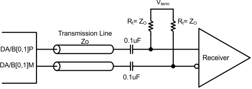 Figure 81. CML Output Connections
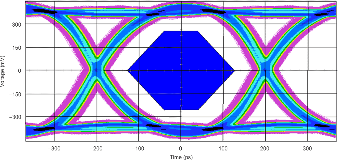
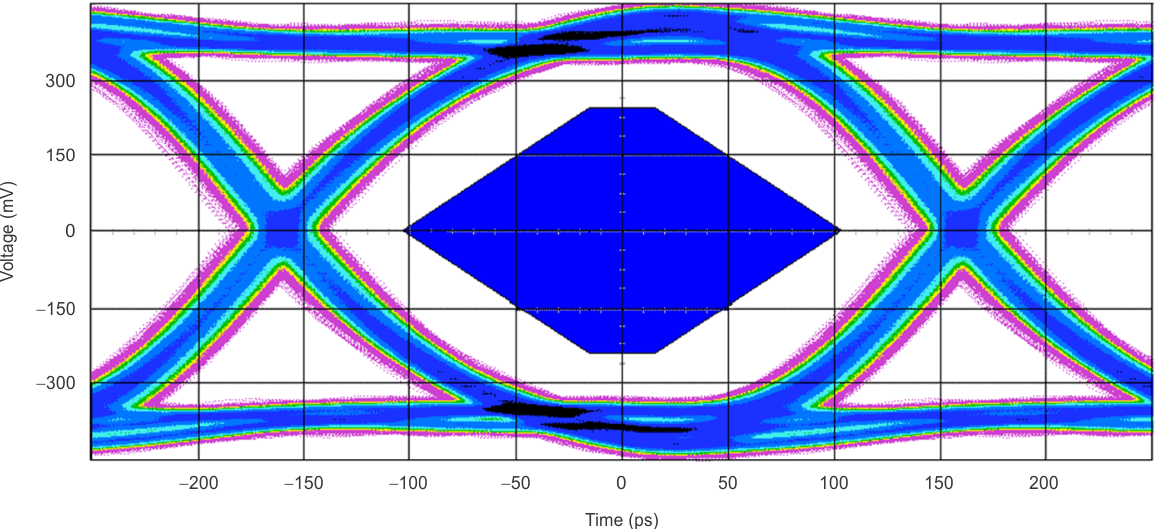
Figure 82 and Figure 83 show the data eye measurements of the device JESD204B transmitter against the JESD204B transmitter mask at 2.5 GBPS (10x mode) and 3.125 GBPS (20x mode), respectively.
9.5 Programming
9.5.1 Device Configuration
The ADS42JB49 and ADS42JB69 can be configured using a serial programming interface, as described in the Serial Interface section. In addition, the device has four dedicated parallel pins (PDN_GBL, STBY, CTRL1, and CTRL2) for controlling the power-down modes.
9.5.2 Details of Serial Interface
The ADC has a set of internal registers that can be accessed by the serial interface formed by the SEN (serial interface enable), SCLK (serial interface clock), SDATA (serial interface data), and SDOUT (serial interface data output) pins. Serially shifting bits into the device is enabled when SEN is low. SDATA serial data are latched at every SCLK rising edge when SEN is active (low). The serial data are loaded into the register at every 16th SCLK rising edge when SEN is low. When the word length exceeds a multiple of 16 bits, the excess bits are ignored. Data can be loaded in multiples of 16-bit words within a single active SEN pulse. The interface functions with SCLK frequencies from 20 MHz down to very low speeds (of a few hertz) and also with non-50% SCLK duty cycle.
9.5.2.1 Register Initialization
After power-up, the internal registers must be initialized to their default values through a hardware reset by applying a high pulse on the RESET pin (of widths greater than 10 ns), as shown in Figure 84. Later during operation, if required serial interface registers can be cleared by:
- Either through a hardware reset or
- By applying a software reset. When using the serial interface, set the RESET bit (D0 in register address 08h) high. This setting initializes the internal registers to the default values and then self-resets the RESET bit low. In this case, the RESET pin is kept low.
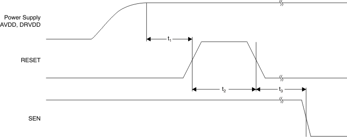
Table 11. Reset Timing (1)
| TEST CONDITIONS | MIN | TYP | MAX | UNIT | ||
|---|---|---|---|---|---|---|
| t1 | Power-on delay | Delay from AVDD and DRVDD power-up to active RESET pulse | 1 | ms | ||
| t2 | Reset pulse width | Active RESET signal pulse width | 10 | ns | ||
| 1 | µs | |||||
| t3 | Register write delay | Delay from RESET disable to SEN active | 100 | ns | ||
9.5.2.2 Serial Register Write
The internal device register can be programmed following these steps:
- Drive the SEN pin low.
- Set the R/W bit to ‘0’ (bit A7 of the 8-bit address).
- Set bit A6 in the address field to ‘0’.
- Initiate a serial interface cycle specifying the address of the register (A5 to A0) whose content must be written (as shown in Figure 85 and Table 12).
- Write the 8-bit data that is latched on the SCLK rising edge.
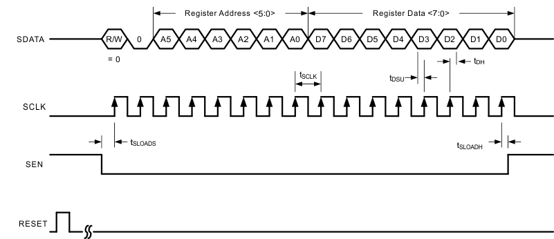 Figure 85. Serial Register Write Timing Diagram
Table 12. Serial Interface Timing(1)
| MIN | TYP | MAX | UNIT | ||
|---|---|---|---|---|---|
| fSCLK | SCLK frequency (equal to 1 / tSCLK) | > dc | 20 | MHz | |
| tSLOADS | SEN to SCLK setup time | 25 | ns | ||
| tSLOADH | SCLK to SEN hold time | 25 | ns | ||
| tDSU | SDIO setup time | 25 | ns | ||
| tDH | SDIO hold time | 25 | ns | ||
9.5.2.3 Serial Register Readout
The device includes a mode where the contents of the internal registers can be read back. This readback mode may be useful as a diagnostic check to verify the serial interface communication between the external controller and the ADC.
- Set bit A7 (MSB) of 8 bit address to '1'.
- Write the address of register on bits A5 through A0 whose contents must be read. See Figure 86
- The device outputs the contents (D7 to D0) of the selected register on the SDOUT pin (pin 45).
- The external controller can latch the contents at the SCLK rising edge.
When serial registers are enabled for writing (bit A7 of 8-bit address bus is 0), the SDOUT pin is in a high-impedance mode. If serial readout is not used, the SDOUT pin must float. Figure 86 shows a timing diagram of this readout mode. SDOUT comes out at the SCLK falling edge with an approximate delay (tSD_DELAY) of 20 ns, as shown in Figure 87.
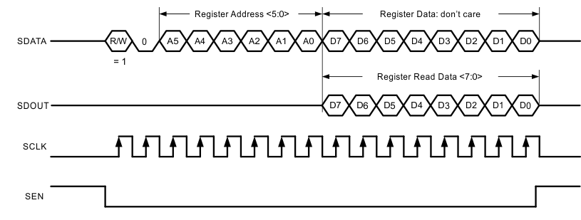 Figure 86. Serial Register Readout Timing Diagram
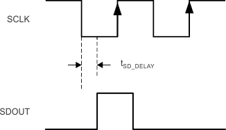 Figure 87. SDOUT Timing Diagram
9.6 Register Maps
Table 13 lists a summary of the serial interface registers.
Table 13. Summary of Serial Interface Registers
Table 14. High-Frequency Modes Summary
| REGISTER ADDRESS | VALUE | DESCRIPTION |
|---|---|---|
| Dh | 90h | High-frequency modes should be enabled for input frequencies greater than 250 MHz. |
| Eh | 90h | High-frequency modes should be enabled for input frequencies greater than 250 MHz. |
9.6.1 Description of Serial Interface Registers
9.6.1.1 Register 6 (offset = 06h) [reset = 00h]
| D7 | D6 | D5 | D4 | D3 | D2 | D1 | D0 |
| 0 | 0 | 0 | 0 | 0 | 0 | CLK DIV | |
| W-0h | W-0h | W-0h | W-0h | W-0h | W-0h | R/W-0h | |
| LEGEND: R/W = Read/Write; R = Read only; -n = value after reset |
Table 15. Register 6 Field Descriptions
| Bit | Field | Type | Reset | Description |
|---|---|---|---|---|
| D[7:2] | 0 | W | 0h | Always write '0' |
| D[1:0] | CLK DIV | R/W | 0h | Internal clock divider for input sample clock 00 : Divide-by-1 (clock divider bypassed) 01 : Divide-by-2 10 : Divide-by-1 11 : Divide-by-4 |
9.6.1.2 Register 7 (offset = 07h) [reset = 00h]
| D7 | D6 | D5 | D4 | D3 | D2 | D1 | D0 |
| 0 | 0 | 0 | 0 | 0 | 0 | SYSREF DELAY | |
| W-0h | W-0h | W-0h | W-0h | W-0h | W-0h | R/W-0h | |
| LEGEND: R/W = Read/Write; R = Read only; -n = value after reset |
Table 16. Register 7 Field Descriptions
| Bit | Field | Type | Reset | Description |
|---|---|---|---|---|
| D[7:2] | 0 | W | 0h | Always write '0' |
| D[1:0] | SYSREF DELAY | R/W | 0h | Controls the delay of the SYSREF input with respect to the input clock. Typical values for the expected delay of different settings are: 000 : 0-ps delay 001 : 60-ps delay 010 : 120-ps delay 011 : 180-ps delay 100 : 240-ps delay 101 : 300-ps delay 110 : 360-ps delay 111 : 420-ps delay |
9.6.1.3 Register 8 (offset = 08h) [reset = 00h]
| D7 | D6 | D5 | D4 | D3 | D2 | D1 | D0 |
| PDN CHA | PDN CHB | STDBY | DATA FORMAT | 1 | 0 | 0 | RESET |
| R/W-0h | R/W-0h | R/W-0h | R/W-0h | W-1h | W-0h | W-0h | R/W-0h |
| LEGEND: R/W = Read/Write; R = Read only; -n = value after reset |
Table 17. Register 8 Field Descriptions
| Bit | Field | Type | Reset | Description |
|---|---|---|---|---|
| D7 | PDN CHA | R/W | 0h | Power-down channel A 0 : Normal operation 1 : Channel A power-down |
| D6 | PDN CHB | R/W | 0h | Power-down channel B 0 : Normal operation 1 : Channel B power-down |
| D5 | STBY | R/W | 0h | Dual ADC is placed into standby mode 0 : Normal operation 1 : Both ADCs are powered down (input clock buffer and CML output buffers are alive) |
| D4 | DATA FORMAT | R/W | 0h | Digital output data format 0 : Twos complement 1 : Offset binary |
| D3 | 1 | W | 1h | Always write '1' Default value of this bit is '0'. This bit must always be set to '1'. |
| D[2:1] | 0 | W | 0h | Always write '0' |
| D0 | RESET | R/W | 0h | Software reset applied This bit resets all internal registers to the default values and self-clears to ‘0’. |
9.6.1.4 Register B (offset = 0Bh) [reset = 00h]
| D7 | D6 | D5 | D4 | D3 | D2 | D1 | D0 |
| CHA GAIN | CHA GAIN EN | 0 | 0 | ||||
| R/W-0h | R/W-0h | W-0h | W-0h | ||||
| LEGEND: R/W = Read/Write; R = Read only; -n = value after reset |
Table 18. Register B Field Descriptions
| Bit | Field | Type | Reset | Description |
|---|---|---|---|---|
| D[7:3] | CHA GAIN | R/W | 0h | Digital gain for channel A (must set the CHA GAIN EN bit first, bit D2). Bit descriptions are listed in Table 19. |
| D2 | CHA GAIN EN | R/W | 0h | Digital gain enable bit for channel A 0 : Digital gain disabled 1 : Digital gain enabled |
| D[1:0] | 0 | W | 0h | Always write '0' |
Table 19. Digital Gain for Channel A
| REGISTER VALUE | DIGITAL GAIN | FULL-SCALE INPUT VOLTAGE | REGISTER VALUE | DIGITAL GAIN | FULL-SCALE INPUT VOLTAGE | |
|---|---|---|---|---|---|---|
| 00000 | 0 dB | 2.0 VPP | 01010 | 1.5 dB | 1.7 VPP | |
| 00001 | Do not use | — | 01011 | 2 dB | 1.6 VPP | |
| 00010 | Do not use | — | 01100 | 2.5 dB | 1.5 VPP | |
| 00011 | –2.0 dB | 2.5 VPP | 01101 | 3 dB | 1.4 VPP | |
| 00100 | –1.5 dB | 2.4 VPP | 01110 | 3.5 dB | 1.3 VPP | |
| 00101 | –1.0 dB | 2.2 VPP | 01111 | 4 dB | 1.25 VPP | |
| 00110 | –0.5 dB | 2.1 VPP | 10000 | 4.5 dB | 1.2 VPP | |
| 00111 | 0 dB | 2.0 VPP | 10001 | 5 dB | 1.1 VPP | |
| 01000 | 0.5 dB | 1.9 VPP | 10010 | 5.5 dB | 1.05 VPP | |
| 01001 | 1 dB | 1.8 VPP | 10011 | 6 dB | 1.0 VPP |
9.6.1.5 Register C (offset = 0Ch) [reset = 00h]
| D7 | D6 | D5 | D4 | D3 | D2 | D1 | D0 |
| CHB GAIN | CHB GAIN EN | 0 | 0 | ||||
| R/W-0h | R/W-0h | W-0h | W-0h | ||||
| LEGEND: R/W = Read/Write; R = Read only; -n = value after reset |
Table 20. Register C Field Descriptions
| Bit | Field | Type | Reset | Description |
|---|---|---|---|---|
| D[7:3] | CHB GAIN | R/W | 0h | Digital gain for channel B (must set the CHA GAIN EN bit first, bit D2). Bit descriptions are listed in Table 21. |
| D2 | CHB GAIN EN | R/W | 0h | Digital gain enable bit for channel B 0 : Digital gain disabled 1 : Digital gain enabled |
| D[1:0] | 0 | W | 0h | Always write '0' |
Table 21. Digital Gain for Channel B
| REGISTER VALUE | DIGITAL GAIN | FULL-SCALE INPUT VOLTAGE | REGISTER VALUE | DIGITAL GAIN | FULL-SCALE INPUT VOLTAGE | |
|---|---|---|---|---|---|---|
| 00000 | 0 dB | 2.0 VPP | 01010 | 1.5 dB | 1.7 VPP | |
| 00001 | Do not use | — | 01011 | 2 dB | 1.6 VPP | |
| 00010 | Do not use | — | 01100 | 2.5 dB | 1.5 VPP | |
| 00011 | –2.0 dB | 2.5 VPP | 01101 | 3 dB | 1.4 VPP | |
| 00100 | –1.5 dB | 2.4 VPP | 01110 | 3.5 dB | 1.3 VPP | |
| 00101 | –1.0 dB | 2.2 VPP | 01111 | 4 dB | 1.25 VPP | |
| 00110 | –0.5 dB | 2.1 VPP | 10000 | 4.5 dB | 1.2 VPP | |
| 00111 | 0 dB | 2.0 VPP | 10001 | 5 dB | 1.1 VPP | |
| 01000 | 0.5 dB | 1.9 VPP | 10010 | 5.5 dB | 1.05 VPP | |
| 01001 | 1 dB | 1.8 VPP | 10011 | 6 dB | 1.0 VPP |
9.6.1.6 Register D (offset = 0Dh) [reset = 00h]
| D7 | D6 | D5 | D4 | D3 | D2 | D1 | D0 |
| HIGH FREQ 1 | 0 | 0 | HIGH FREQ 1 | 0 | 0 | 0 | FAST OVR EN |
| R/W-0h | W-0h | W-0h | R/W-0h | W-0h | W-0h | W-0h | R/W-0h |
| LEGEND: R/W = Read/Write; R = Read only; -n = value after reset |
Table 22. Register D Field Descriptions
| Bit | Field | Type | Reset | Description |
|---|---|---|---|---|
| D7 | HIGH FREQ 1 | R/W | 0h | High-frequency mode 1 00 : Default 11 : Use for input frequencies > 250 MHz along with HIGH FREQ 2 |
| D[6:5] | 0 | W | 0h | Always write '0' |
| D4 | HIGH FREQ 1 | R/W | 0h | High-frequency mode 1 00 : Default 11 : Use for input frequencies > 250 MHz along with HIGH FREQ 2 |
| D[3:1] | 0 | W | 0h | Always write '0' |
| D0 | FAST OVR EN | R/W | 0h | Selects if normal or fast OVR signal is presented on OVRA, OVRB pins 0 : Normal OVR on OVRA, OVRB pins 1 : Fast OVR on OVRA, OVRB pins |
9.6.1.7 Register E (offset = 0Eh) [reset = 00h]
| D7 | D6 | D5 | D4 | D3 | D2 | D1 | D0 |
| HIGH FREQ 2 | 0 | 0 | HIGH FREQ 2 | 0 | 0 | 0 | 0 |
| R/W-0h | W-0h | W-0h | R/W-0h | W-0h | W-0h | W-0h | W-0h |
| LEGEND: R/W = Read/Write; R = Read only; -n = value after reset |
Table 23. Register E Field Descriptions
| Bit | Field | Type | Reset | Description |
|---|---|---|---|---|
| D7 | HIGH FREQ 2 | R/W | 0h | High-frequency mode 2 00 : Default 11 : Use for input frequencies > 250 MHz along with HIGH FREQ 1 |
| D[6:5] | 0 | W | 0h | Always write '0' |
| D4 | HIGH FREQ 2 | R/W | 0h | High-frequency mode 2 00 : Default 11 : Use for input frequencies > 250 MHz along with HIGH FREQ 1 |
| D[3:0] | 0 | W | 0h | Always write '0' |
9.6.1.8 Register F (offset = 0Fh) [reset = 00h]
| D7 | D6 | D5 | D4 | D3 | D2 | D1 | D0 |
| CHA TEST PATTERNS | CHB TEST PATTERNS | ||||||
| R/W-0h | R/W-0h | ||||||
| LEGEND: R/W = Read/Write; R = Read only; -n = value after reset |
Table 24. Register F Field Descriptions
| Bit | Field | Type | Reset | Description |
|---|---|---|---|---|
| D[7:4] | CHA TEST PATTERNS | R/W | 0h | Channel A test pattern programmability The 16-bit test pattern data are selected as an input to the JESD block (in the ADS42JB49, the last two LSBs of the 16-bit data are replaced by 00). 0000 : Normal operation 0001 : All '0's 0010 : All '1's 0011 : Toggle pattern: In the ADS42JB69, data are an alternating sequence of 1010101010101010 and 0101010101010101. In the ADS42JB49, data alternate between 10101010101010 and 01010101010101. 0100 : Digital ramp: In the ADS42JB69, data increment by 1 LSB every clock cycle from code 0 to 65535. In the ADS42JB49, data increment by 1 LSB every 4th clock cycle from code 0 to 16383. 0101 : Do not use 0110 : Single pattern: In the ADS42JB69, data are the same as programmed by the CUSTOM PATTERN 1[15:0] registers bits. In the ADS42JB49, data are the same as programmed by the CUSTOM PATTERN 1[15:2] register bits. 0111 : Double pattern: In the ADS42JB69, data alternate between CUSTOM PATTERN 1[15:0] and CUSTOM PATTERN 2[15:0]. In the ADS42JB49 data alternate between CUSTOM PATTERN 1[15:2] and CUSTOM PATTERN 2[15:2]. 1000 : Deskew pattern: In the ADS42JB69, data are AAAAh. In the ADS42JB49, data are 3AAAh. 1001 : Do not use 1010 : PRBS pattern: Data are a sequence of pseudo random numbers. 1011 : 8-point sine wave: In the ADS42JB69, data are a repetitive sequence of the following eight numbers, forming a sine-wave in twos complement format: 1, 9598, 32768, 55938, 65535, 55938, 32768, 9598. In the ADS42JB49, data are a repetitive sequence of the following eight numbers, forming a sine-wave in twos complement format: 0, 2399, 8192, 13984, 16383, 13984, 8192, 2399. |
| D[3:0] | CHB TEST PATTERNS | R/W | 0h | Channel B test pattern programmability 16-bit test pattern data are selected as an input to the JESD block (in the ADS42JB49, the last two LSBs of the 16-bit data are replaced by 00). 0000 : Normal operation 0001 : All '0's 0010 : All '1's 0011 : Toggle pattern: In the ADS42JB69, data are an alternating sequence of 1010101010101010 and 0101010101010101. In the ADS42JB49, data alternate between 10101010101010 and 01010101010101. 0100 : Digital ramp: In the ADS42JB69, data increment by 1 LSB every clock cycle from code 0 to 65535. In the ADS42JB49, data increment by 1 LSB every 4th clock cycle from code 0 to 16383. 0101 : Do not use 0110 : Single pattern: In the ADS42JB69, data are the same as programmed by the CUSTOM PATTERN 1[15:0] registers bits. In the ADS42JB49, data are the same as programmed by the CUSTOM PATTERN 1[15:2] register bits. 0111 : Double pattern: In the ADS42JB69, data alternate between CUSTOM PATTERN 1[15:0] and CUSTOM PATTERN 2[15:0]. In the ADS42JB49, data alternate between CUSTOM PATTERN 1[15:2] and CUSTOM PATTERN 2[15:2]. 1000 : Deskew pattern: In the ADS42JB69, data are AAAAh. In the ADS42JB49, data are 3AAAh. 1001 : Do not use 1010 : PRBS pattern: Data are a sequence of pseudo random numbers. 1011 : 8-point sine wave: In the ADS42JB69, data are a repetitive sequence of the following eight numbers, forming a sine-wave in twos complement format: 1, 9598, 32768, 55938, 65535, 55938, 32768, 9598. In the ADS42JB49, data are a repetitive sequence of the following eight numbers, forming a sine-wave in twos complement format: 0, 2399, 8192, 13984, 16383, 13984, 8192, 2399. |
9.6.1.9 Register 10 (offset = 10h) [reset = 00h]
| D7 | D6 | D5 | D4 | D3 | D2 | D1 | D0 |
| CUSTOM PATTERN 1[15:8] | |||||||
| R/W-0h | |||||||
| LEGEND: R/W = Read/Write; R = Read only; -n = value after reset |
Table 25. Register 10 Field Descriptions
| Bit | Field | Type | Reset | Description |
|---|---|---|---|---|
| D[7:0] | CUSTOM PATTERN 1[15:8] | R/W | 0h | Sets CUSTOM PATTERN 1[15:8] using these bits for both channels |
9.6.1.10 Register 11 (offset = 11h) [reset = 00h]
| D7 | D6 | D5 | D4 | D3 | D2 | D1 | D0 |
| CUSTOM PATTERN 1[7:0] | |||||||
| R/W-0h | |||||||
| LEGEND: R/W = Read/Write; R = Read only; -n = value after reset |
Table 26. Register 11 Field Descriptions
| Bit | Field | Type | Reset | Description |
|---|---|---|---|---|
| D[7:0] | CUSTOM PATTERN 1[7:0] | R/W | 0h | Sets CUSTOM PATTERN 1[7:0] using these bits for both channels |
9.6.1.11 Register 12 (offset = 12h) [reset = 00h]
| D7 | D6 | D5 | D4 | D3 | D2 | D1 | D0 |
| CUSTOM PATTERN 2[15:8] | |||||||
| R/W-0h | |||||||
| LEGEND: R/W = Read/Write; R = Read only; -n = value after reset |
Table 27. Register 12 Field Descriptions
| Bit | Field | Type | Reset | Description |
|---|---|---|---|---|
| D[7:0] | CUSTOM PATTERN 2[15:8] | R/W | 0h | Sets CUSTOM PATTERN 2[15:8] using these bits for both channels |
9.6.1.12 Register 13 (offset = 13h) [reset = 00h]
| D7 | D6 | D5 | D4 | D3 | D2 | D1 | D0 |
| CUSTOM PATTERN 2[7:0] | |||||||
| R/W-0h | |||||||
| LEGEND: R/W = Read/Write; R = Read only; -n = value after reset |
Table 28. Register 13 Field Descriptions
| Bit | Field | Type | Reset | Description |
|---|---|---|---|---|
| D[7:0] | CUSTOM PATTERN 2[7:0] | R/W | 0h | Sets CUSTOM PATTERN 2[7:0] using these bits for both channels |
9.6.1.13 Register 1F (offset = 1Fh) [reset = FFh]
| D7 | D6 | D5 | D4 | D3 | D2 | D1 | D0 |
| 0 | FAST OVR THRESHOLD | ||||||
| W-1h | R/W-0h | ||||||
| LEGEND: R/W = Read/Write; R = Read only; -n = value after reset |
Table 29. Register 1F Field Descriptions
| Bit | Field | Type | Reset | Description |
|---|---|---|---|---|
| D7 | 0 | W | W-1h | Always write '0' The default value of this bit is '1'. Always write this bit to '0' when fast OVR thresholds are programmed. |
| D[6:0] | FAST OVR THRESHOLD | R/W | 0h | The device has a fast OVR mode that indicates an overload condition at the ADC input. The input voltage level at which the overload is detected is referred to as the threshold and is programmable using the FAST OVR THRESHOLD bits. FAST OVR is triggered nine output clock cycles after the overload condition occurs. The threshold at which fast OVR is triggered is (full-scale × [the decimal value of the FAST OVR THRESHOLD bits] / 127). See the Overrange Indication section for details. |
9.6.1.14 Register 26 (offset = 26h) [reset = 00h]
| D7 | D6 | D5 | D4 | D3 | D2 | D1 | D0 |
| SERDES TEST PATTERN | IDLE SYNC | TESTMODE EN | FLIP ADC DATA | LANE ALIGN | FRANE ALIGN | TX LINK CONFIG DATA | |
| R/W-0h | R/W-0h | R/W-0h | R/W-0h | R/W-0h | R/W-0h | R/W-0h | |
| LEGEND: R/W = Read/Write; R = Read only; -n = value after reset |
Table 30. Register 26 Field Descriptions
| Bit | Field | Type | Reset | Description |
|---|---|---|---|---|
| D[7:6] | SERDES TEST PATTERN | R/W | 0h | Sets test patterns in the transport layer of the JESD204B interface 00 : Normal operation 01 : Outputs clock pattern: Output is a 10101010 pattern 10 : Encoded pattern: Output is 1111111100000000 11 : PRBS sequence: Output is 215 – 1 |
| D5 | IDLE SYNC | R/W | 0h | Sets output pattern when SYNC~ is asserted 0 : Sync code is k28.5 (0xBCBC) 1 : Sync code is 0xBC50 |
| D4 | TESTMODE EN | R/W | 0h | Generates a long transport layer test pattern mode according to the 5.1.63 clause of the JESD204B specification 0 : Test mode disabled 1 : Test mode enabled |
| D3 | FLIP ADC DATA | R/W | 0h | 0 : Normal operation 1 : Output data order is reversed: MSB – LSB |
| D2 | LANE ALIGN | R/W | 0h | Inserts a lane alignment character (K28.3) for the receiver to align to the lane boundary per section 5.3.3.5 of the JESD204B specification. 0 : Lane alignment characters are not inserted. 1 : Inserts lane alignment characters |
| D1 | FRAME ALIGN | R/W | 0h | Inserts a frame alignment character (K28.7) for the receiver to align to the frame boundary per section 5.3.3.4 of the JESD204B specification. 0 : Frame alignment characters are not inserted. 1 : Inserts frame alignment characters |
| D0 | TX LINK CONFIG DATA | R/W | 0h | Disables sending initial link alignment (ILA) sequence when SYNC~ is de-asserted, '0' 0 : ILA enabled 1 : ILA disabled |
9.6.1.15 Register 27 (offset = 27h) [reset = 00h]
| D7 | D6 | D5 | D4 | D3 | D2 | D1 | D0 |
| 0 | 0 | 0 | 0 | 0 | 0 | CTRL K | CTRL F |
| W-0h | W-0h | W-0h | W-0h | W-0h | W-0h | R/W-0h | R/W-0h |
| LEGEND: R/W = Read/Write; R = Read only; -n = value after reset |
Table 31. Register 27 Field Descriptions
| Bit | Field | Type | Reset | Description |
|---|---|---|---|---|
| D[7:2] | 0 | W | 0h | Always write '0' |
| D1 | CTRL K | R/W | 0h | Enables bit for number of frames per multiframe 0 : Default 1 : Frames per multiframe can be set in register 2Dh |
| D0 | CTRL F | R/W | 0h | Enables bit for number of octets per frame 0 : Default 1 : Octets per frame can be specified in register 2Ch |
9.6.1.16 Register 2B (offset = 2Bh) [reset = 00h]
| D7 | D6 | D5 | D4 | D3 | D2 | D1 | D0 |
| SCRAMBLE EN | 0 | 0 | 0 | 0 | 0 | 0 | 0 |
| R/W-0h | W-0h | W-0h | W-0h | W-0h | W-0h | W-0h | W-0h |
| LEGEND: R/W = Read/Write; R = Read only; -n = value after reset |
Table 32. Register 2B Field Descriptions
| Bit | Field | Type | Reset | Description |
|---|---|---|---|---|
| D7 | SCRAMBLE EN | R/W | 0h | Scramble enable bit in the JESD204B interface 0 : Scrambling disabled 1 : Scrambling enabled |
| D[6:0] | 0 | W | 0h | Always write '0' |
9.6.1.17 Register 2C (offset = 2Ch) [reset = 00h]
| D7 | D6 | D5 | D4 | D3 | D2 | D1 | D0 |
| 0 | 0 | 0 | 0 | 0 | 0 | 0 | OCTETS PER FRAME |
| W-0h | W-0h | W-0h | W-0h | W-0h | W-0h | W-0h | R/W-0h |
| LEGEND: R/W = Read/Write; R = Read only; -n = value after reset |
Table 33. Register 2C Field Descriptions
| Bit | Field | Type | Reset | Description |
|---|---|---|---|---|
| D[7:1] | 0 | W | 0h | Always write '0' |
| D0 | OCTETS PER FRAME | R/W | 0h | Sets number of octets per frame (F) 0 : 10x mode using two lanes per ADC 1 : 20x mode using one lane per ADC |
9.6.1.18 Register 2D (offset = 2Dh) [reset = 00h]
| D7 | D6 | D5 | D4 | D3 | D2 | D1 | D0 |
| 0 | 0 | 0 | FRAMES PER MULTIFRAME | ||||
| W-0h | W-0h | W-0h | R/W-0h | ||||
| LEGEND: R/W = Read/Write; R = Read only; -n = value after reset |
Table 34. Register 2D Field Descriptions
| Bit | Field | Type | Reset | Description |
|---|---|---|---|---|
| D[7:5] | 0 | W | 0h | Always write '0' |
| D[4:0] | FRAMES PER MULTIFRAME | R/W | 0h | Sets number of frames per multiframe After reset, the default settings for frames per multiframe are: 10x : K = 16 20x : K = 8 For each mode, K must not be set to a lower value. |
9.6.1.19 Register 30 (offset = 30h) [reset = 40h]
| D7 | D6 | D5 | D4 | D3 | D2 | D1 | D0 |
| SUBCLASS | 0 | 0 | 0 | 0 | 0 | ||
| R/W-0h | W-0h | W-0h | W-0h | W-0h | W-0h | ||
| LEGEND: R/W = Read/Write; R = Read only; -n = value after reset |
Table 35. Register 30 Field Descriptions
| Bit | Field | Type | Reset | Description |
|---|---|---|---|---|
| D[7:5] | SUBCLASS | R/W | 0h | Sets JESD204B subclass. Note that the default value of these bits after reset is 010, which makes subclass 2 the default class. 000 : Subclass 0. Backward compatibility with JESD204A. 001 : Subclass 1. Deterministic latency using the SYSREF signal. 010 : Subclass 2. Deterministic latency using SYNC~ detection (default subclass after reset). |
| D[4:0] | 0 | W | 0h | Always write '0' |
9.6.1.20 Register 36 (offset = 36h) [reset = 00h]
| D7 | D6 | D5 | D4 | D3 | D2 | D1 | D0 |
| SYNC REQ | LMFC RESET MASK | 0 | 0 | OUTPUT CURRENT SEL | |||
| R/W-0h | R/W-0h | W-0h | W-0h | R/W-0h | |||
| LEGEND: R/W = Read/Write; R = Read only; -n = value after reset |
Table 36. Register 36 Field Descriptions
| Bit | Field | Type | Reset | Description |
|---|---|---|---|---|
| D7 | SYNC REQ | R/W | 0h | Generates synchronization request 0 : Normal operation 1 : Generates sync request |
| D6 | LMFC RESET MASK | R/W | 0h | Mask LMFC reset coming to digital 0 : LMFC reset is not masked 1 : Ignores LMFC reset |
| D[5:4] | 0 | W | 0h | Always write '0' |
| D[3:0] | OUTPUT CURRENT SEL | R/W | 0h | Changes JESD output buffer current 0000 : 16 mA 0001 : 15 mA 0010 : 14 mA 0011 : 13 mA 0100 : 20 mA 0101 : 19 mA 0110 : 18 mA 0111 : 17 mA 1000 : 8 mA 1001 : 7 mA 1010 : 6 mA 1011 : 5 mA 1100 : 12 mA 1101 : 11 mA 1110 : 10 mA 1111 : 9 mA |
9.6.1.21 Register 37 (offset = 37h) [reset = 00h]
| D7 | D6 | D5 | D4 | D3 | D2 | D1 | D0 |
| LINK LAYER TESTMODE | LINK LAYER RPAT | 0 | PULSE DET MODES | ||||
| R/W-0h | R/W-0h | W-0h | R/W-0h | ||||
| LEGEND: R/W = Read/Write; R = Read only; -n = value after reset |
Table 37. Register 37 Field Descriptions
| Bit | Field | Type | Reset | Description |
|---|---|---|---|---|
| D[7:5] | LINK LAYER TESTMODE | R/W | 0h | Generates a pattern according to clause 5.3.3.8.2 of the JESD204B document 000 : Normal ADC data 001 : D21.5 (high-frequency jitter pattern) 010 : K28.5 (mixed-frequency jitter pattern) 011 : Repeats initial lane alignment (generates a K28.5 character and repeats lane alignment sequences continuously) 100 : 12-octet RPAT jitter pattern |
| D4 | LINK LAYER RPAT | R/W | 0h | Changes the running disparity in modified RPAT pattern test mode (only when link layer test mode = 100) 0 : Normal operation 1 : Changes disparity |
| D3 | 0 | W | 0h | Always write '0' |
| D[2:0] | PULSE DET MODES | R/W | 0h | Selects different detection modes for SYSREF (subclass 1) and SYNC (subclass 2) |
| D2 | D1 | D0 | FUNCTIONALITY |
|---|---|---|---|
| 0 | Don’t care | 0 | Allows all pulses to reset input clock dividers |
| 1 | Don’t care | 0 | Do not allow reset of analog clock dividers |
| Don’t care | 0 to 1 transition | 1 | Allows one pulse immediately after the 0 to 1 transition to reset the divider |
9.6.1.22 Register 38 (offset = 38h) [reset = 00h]
| D7 | D6 | D5 | D4 | D3 | D2 | D1 | D0 |
| FORCE LMFC COUNT | LMFC COUNT INIT | RELEASE ILANE SEQ | |||||
| R/W-0h | R/W-0h | R/W-0h | |||||
| LEGEND: R/W = Read/Write; R = Read only; -n = value after reset |
Table 38. Register 38 Field Descriptions
| Bit | Field | Type | Reset | Description |
|---|---|---|---|---|
| D7 | FORCE LMFC COUNT | R/W | 0h | Forces LMFC count 0 : Normal operation 1 : Enables using a different starting value for the LMFC counter |
| D[6:2] | LMFC COUNT INIT | R/W | 0h | SYSREF receives the digital block and resets the LMFC count to '0'. K28.5 stops transmitting when the LMFC count reaches 31. The initial value that the LMFC count resets to can be set using LMFC COUNT INIT. In this manner, the Rx can be synchronized early because the Rx gets the LANE ALIGNMENT SEQUENCE early. The FORCE LMFC COUNT register bit must be enabled. |
| D[1:0] | RELEASE ILANE SEQ | R/W | 0h | Delays the generation of the lane alignment sequence by 0, 1, 2, or 3 multiframes after the code group synchronization. 00 : 0 01 : 1 10 : 2 11 : 3 |