SLAS669E September 2010 – may 2020 ADS5400-SP
PRODUCTION DATA.
- 1 Features
- 2 Applications
- 3 Description
- 4 Revision History
- 5 Pin Configuration and Functions
- 6 Specifications
-
7 Detailed Description
- 7.1 Overview
- 7.2 Functional Block Diagram
- 7.3 Feature Description
- 7.4 Device Functional Modes
- 7.5 Programming
- 7.6 Serial Register Map
- 8 Application and Implementation
- 9 Power Supply Recommendations
- 10Layout
- 11Device and Documentation Support
- 12Mechanical, Packaging, and Orderable Information
Package Options
Mechanical Data (Package|Pins)
- HFS|100
Thermal pad, mechanical data (Package|Pins)
Orderable Information
7.3.4 Clock Inputs
The ADS5400-SP clock input can be driven with either a differential clock signal or a single-ended clock input. The equivalent clock input circuit can be seen in Figure 28. In low-input-frequency applications, where jitter may not be a big concern, the use of a single-ended clock (as shown in Figure 29) could save cost and board space without much performance tradeoff. When clocked with this configuration, it is best to connect CLK to ground with a 0.01-μF capacitor, while CLK is ac-coupled with a 0.01-μF capacitor to the clock source, as shown in Figure 29.
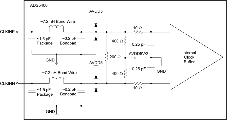 Figure 28. Clock Input Circuit
 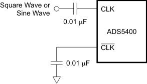 Figure 29. Single-Ended Clock
 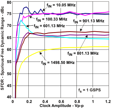 Figure 30. ADS5400 SFDR vs Differential Clock Level
 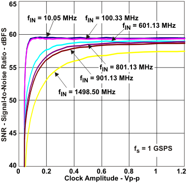 Figure 31. ADS5400 SNR vs Differential Clock Level
 The characterization of the ADS5400-SP is typically performed with a 1.5 VPP differential clock, but the ADC performs well with a differential clock amplitude down to ~400 mVPP (200mV swing on both CLK and CLK), as shown in Figure 30 and Figure 31. For jitter-sensitive applications, the use of a differential clock has some advantages at the system level and is strongly recommended. The differential clock allows for common-mode noise rejection at the printed circuit board (PCB) level. With a differential clock, the signal-to-noise ratio of the ADC is better for jitter-sensitive, high-frequency applications because the board level clock jitter is superior.
Larger clock amplitude levels are recommended for high analog input frequencies or slow clock frequencies. At high analog input frequencies, the sampling process is sensitive to jitter. At slow clock frequencies, a small amplitude sinusoidal clock has a lower slew rate and can create jitter-related SNR degradation due to the uncertainty in the sampling point associated with a slow slew rate. Figure 32 demonstrates a recommended method for converting a single-ended clock source into a differential clock; it is similar to the configuration found on the evaluation board and was used for much of the characterization. See also Clocking High Speed Data Converters (SLYT075) for more details.
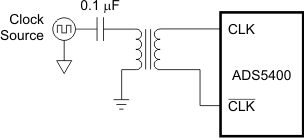 Figure 32. Differential Clock
 The common-mode voltage of the clock inputs is set internally to 2.5 V using internal 400 Ω resistors (see Figure 28). It is recommended to use ac coupling in the clock path, but if this scheme is not possible, the ADS5400-SP features good tolerance to clock common-mode variation, as shown in Figure 33 and Figure 34. The internal ADC core uses both edges of the clock for the conversion process. Ideally, a 50% duty-cycle clock signal should be provided.
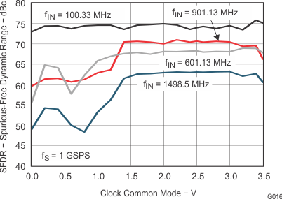 Figure 33. ADS5400-SP SFDR vs Clock Common Mode
 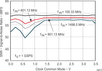 Figure 34. ADS5400-SP SNR vs Clock Common Mode
 To understand how to determine the required clock jitter, an example is useful. The ADS5400 is capable of achieving 58.7 dBFS SNR at 850 MHz of analog input frequency. To achieve SNR at 850 MHz, the external clock source rms jitter must be at least 210fs when combined with the 125fs of internal aperture jitter in order for the total rms jitter to be 244fs. A summary of maximum recommended rms clock jitter as a function of analog input frequency is provided in Table 1 (using 125fs of internal aperture jitter). The equations used to create the table are also presented.
Table 1. Recommended RMS Clock Jitter
| INPUT FREQUENCY
(MHz) |
MEASURED SNR
(dBc) |
TOTAL JITTER
(fs rms) |
MAXIMUM EXT CLOCK JITTER
(fs rms) |
|---|---|---|---|
| 125 | 58.1 | 1585 | 1580 |
| 600 | 57.8 | 318 | 342 |
| 850 | 57.7 | 244 | 210 |
| 1200 | 56.6 | 196 | 151 |
| 1700 | 54.7 | 172 | 119 |
Equation 1 and Equation 2 are used to estimate the required clock source jitter.


where:
jTOTAL = the rms summation of the clock and ADC aperture jitter;
jADC = the ADC internal aperture jitter which is located in the data sheet;
jCLOCK = the rms jitter of the clock at the clock input pins to the ADC; and
fIN = the analog input frequency.
Notice that the SNR is a strong function of the analog input frequency, not the clock frequency. The slope of the clock source edges can have a mild impact on SNR as well and is not taken into account for these estimates. For this reason, maximizing clock source amplitudes at the ADC clock inputs is recommended, though not required (faster slope is desirable for jitter-related SNR). For more information on clocking high-speed ADCs, see Application Note SLWA034, Implementing a CDC7005 Low Jitter Clock Solution For High-Speed, High-IF ADC Devices. Recommended clock distribution chips (CDCs) are the TI CDC7005 and CDCM7005. Depending on the jitter requirements, a band pass filter (BPF) is sometimes required between the CDC and the ADC. If the insertion loss of the BPF causes the clock amplitude to be too low for the ADC, or the clock source amplitude is too low to begin with, an inexpensive amplifier can be placed between the CDC and the BPF.
Figure 35 represents a scenario where an LVPECL output is used from a TI CDCM7005 with the clock signal path optimized for maximum amplitude and minimum jitter. The jitter of this setup is difficult to estimate and requires a careful phase noise analysis of the clock path. The BPF (and possibly a low-cost amplifier because of insertion loss in the BPF) can improve the jitter between the CDC and ADC when the jitter provided by the CDC is still not adequate. The total jitter at the CDCM7005 output depends heavily on the phase noise of the VCXO selected. If it is determined that the jitter from the CDCM7005 with a VCXO is sufficient without further conditioning, it is possible to clock the device directly from the CDCM7005 using differential LVPECL outputs (see the CDCM7005 data sheet for the exact schematic). A careful analysis of the required jitter and of the components involved is recommended before determining the proper approach.
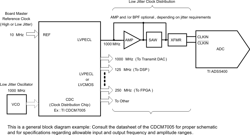 Figure 35. Clock Source Diagram