SLAS669E September 2010 – may 2020 ADS5400-SP
PRODUCTION DATA.
- 1 Features
- 2 Applications
- 3 Description
- 4 Revision History
- 5 Pin Configuration and Functions
- 6 Specifications
-
7 Detailed Description
- 7.1 Overview
- 7.2 Functional Block Diagram
- 7.3 Feature Description
- 7.4 Device Functional Modes
- 7.5 Programming
- 7.6 Serial Register Map
- 8 Application and Implementation
- 9 Power Supply Recommendations
- 10Layout
- 11Device and Documentation Support
- 12Mechanical, Packaging, and Orderable Information
Package Options
Mechanical Data (Package|Pins)
- HFS|100
Thermal pad, mechanical data (Package|Pins)
Orderable Information
6.9 Typical Characteristics
Typical plots at TA = 25°C, sampling rate = 1 GSPS, 50% clock duty cycle, AVDD5 = 5 V, AVDD3 = 3.3 V, DVDD3 = 3.3 V, and 1.5-VPP differential clock, (unless otherwise noted)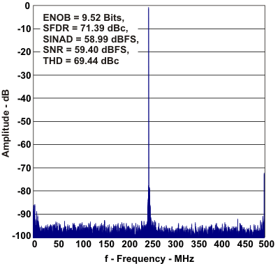 Figure 6. Spectral Performance v FFT for 250-MHz Input Signal
 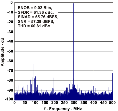 Figure 8. Spectral Performance v FFT for 1.3-GHz Input signal
 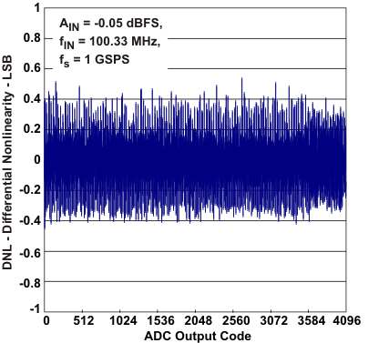 Figure 10. Differential Nonlinearity
 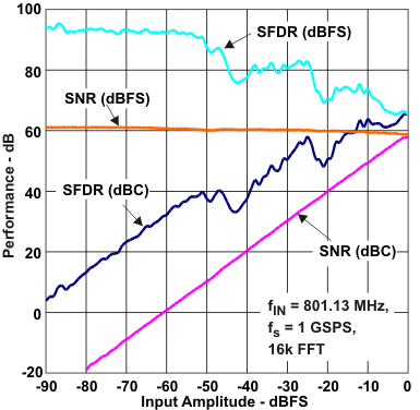 Figure 12. AC Performance vs Input Amplitude (801.13-MHz Input signal)
 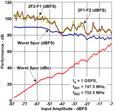 Figure 14. AC Performance vs Input Amplitude (747.5-MHz and 752.5-MHz Two-tone Input Signal)
 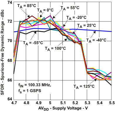 Figure 16. SFDR vs AVDD5 Across Temperature
 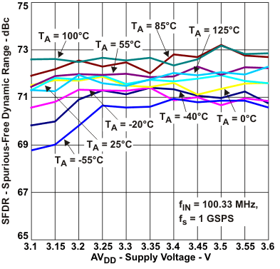 Figure 18. SFDR vs AVDD3 Across Temperature
 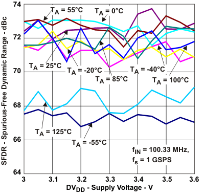 Figure 20. SFDR vs DVDD3 Across Temperature
 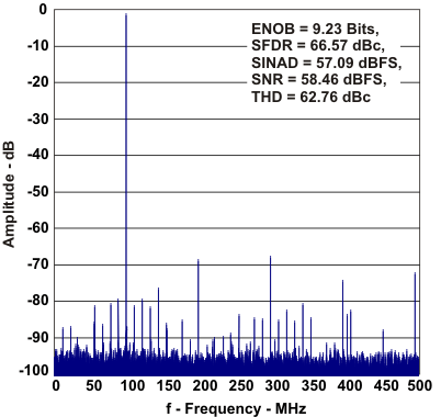 Figure 7. Spectral Performance v FFT for 0.9-GHz Input Signal
 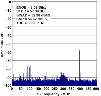 Figure 9. Spectral Performance v FFT for 1.7-GHz Input Signal
 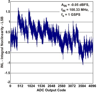 Figure 11. Integral Nonlinearity
 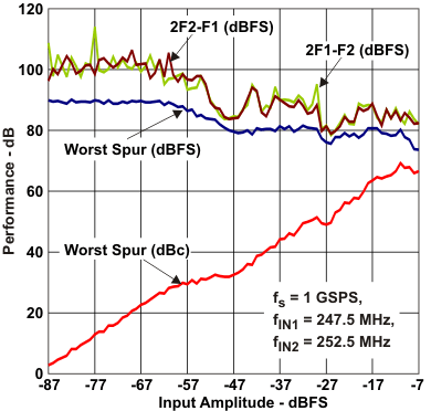 Figure 13. AC Performance vs Input Amplitude (247.5-MHz and 252.5-MHz Two-tone Input Signal)
 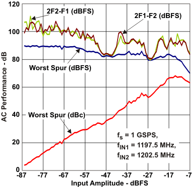 Figure 15. AC Performance vs Input Amplitude (1197.5-MHz and 1202.5-MHz Two-tone Input Signal)
 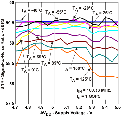 Figure 17. SNR vs AVDD5 Across Temperature
 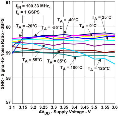 Figure 19. SNR vs AVDD3 Across Temperature
 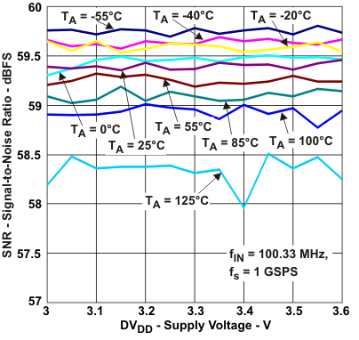 Figure 21. SNR vs DVDD3 Across Temperature
 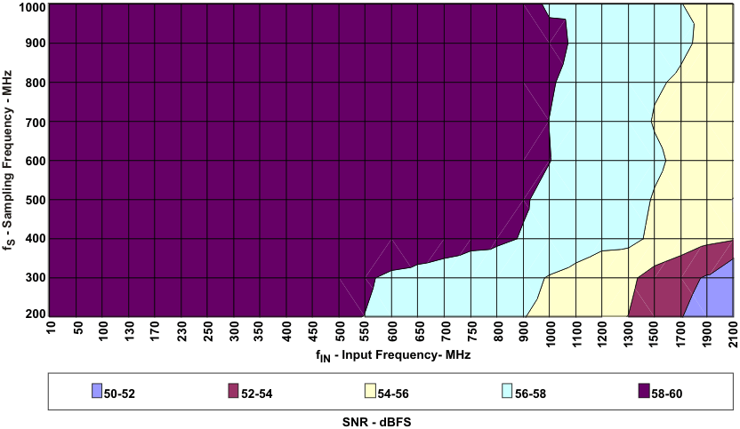 Figure 22. SNR vs Input Frequency and Sampling Frequency
 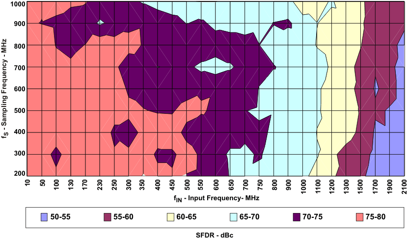 Figure 23. SFDR vs Input Frequency and Sampling Frequency
 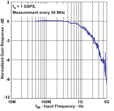 Figure 24. Normalized Gain Response vs Input Frequency