SLAS669E September   2010  – may 2020 ADS5400-SP

PRODUCTION DATA.  

  1. Features
  2. Applications
  3. Description
    1.     Block Diagram
  4. Revision History
  5. Pin Configuration and Functions
    1.     Pin Functions
  6. Specifications
    1. 6.1 Absolute Maximum Ratings
    2. 6.2 ESD Ratings
    3. 6.3 Recommended Operating Conditions
    4. 6.4 Thermal Information
    5. 6.5 Electrical Characteristics
    6. 6.6 Switching Characteristics
    7. 6.7 Timing Characteristics
    8. 6.8 Interleaving Adjustments
    9. 6.9 Typical Characteristics
  7. Detailed Description
    1. 7.1 Overview
    2. 7.2 Functional Block Diagram
    3. 7.3 Feature Description
      1. 7.3.1  Input Configuration
      2. 7.3.2  Voltage Reference
      3. 7.3.3  Analog Input Over-Range Recovery Error
      4. 7.3.4  Clock Inputs
      5. 7.3.5  Over Range
      6. 7.3.6  Data Scramble
      7. 7.3.7  Test Patterns
      8. 7.3.8  Die Identification and Revision
      9. 7.3.9  Die Temperature Sensor
      10. 7.3.10 Interleaving
        1. 7.3.10.1 Gain Adjustment
        2. 7.3.10.2 Offset Adjustment
        3. 7.3.10.3 Input Clock Coarse Phase Adjustment
        4. 7.3.10.4 Input Clock Fine Phase Adjustment
    4. 7.4 Device Functional Modes
      1. 7.4.1 Output Bus and Clock Options
      2. 7.4.2 Reset and Synchronization
      3. 7.4.3 LVDS
    5. 7.5 Programming
      1. 7.5.1 Serial Interface
        1. Table 2. Instruction Byte of the Serial Interface
    6. 7.6 Serial Register Map
      1. 7.6.1 Description of Serial Registers
  8. Application and Implementation
    1. 8.1 Application Information
    2. 8.2 Typical Application
      1. 8.2.1 Design Requirements
      2. 8.2.2 Detailed Design Procedure
        1. 8.2.2.1 Clocking Source for ADS5400-SP
        2. 8.2.2.2 Amplifier Selection
      3. 8.2.3 Application Curve
  9. Power Supply Recommendations
  10. 10Layout
    1. 10.1 Layout Guidelines
    2. 10.2 Layout Example
  11. 11Device and Documentation Support
    1. 11.1 Device Support
      1. 11.1.1 Device Nomenclature
        1. 11.1.1.1 Definition of Specifications
    2. 11.2 Documentation Support
    3. 11.3 Receiving Notification of Documentation Updates
    4. 11.4 Support Resources
    5. 11.5 Trademarks
    6. 11.6 Electrostatic Discharge Caution
    7. 11.7 Glossary
  12. 12Mechanical, Packaging, and Orderable Information

Package Options

Mechanical Data (Package|Pins)
Thermal pad, mechanical data (Package|Pins)
Orderable Information

Description

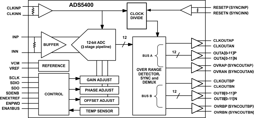
The ADS5400 is a 12-bit, 1-GSPS analog-to-digital converter (ADC) that operates from both a 5-V supply and 3.3-V supply, while providing LVDS-compatible digital outputs. The analog input buffer isolates the internal switching of the track and hold from disturbing the signal source. The simple 3-stage pipeline provides extremely low latency for time critical applications. Designed for the conversion of signals up to 2 GHz of input frequency at 1 GSPS, the ADS5400 has outstanding low noise performance and spurious-free dynamic range over a large input frequency range.

The ADS5400 is available in a 100-Pin Ceramic Nonconductive Tie-Bar Package. The combination of the ceramic package and moderate power consumption of the ADS5400 allows for operation without an external heatsink. The ADS5400 is built on Texas Instrument's complementary bipolar process (BiCom3) and is specified over the full military temperature range (–55°C to 125°C Tcase).

Device Information(1)

PART NUMBER PACKAGE BODY SIZE (NOM)
ADS5400-SP HSF (100) 19.05 mm x 19.05 mm
  1. For all available packages, see the orderable addendum at the end of the data sheet.

Block Diagram
ADS5400-SP fbd_las611.gif