SBAS928C February   2020  – September 2023 ADS7066

PRODUCTION DATA  

  1.   1
  2. Features
  3. Applications
  4. Description
  5. Revision History
  6. Pin Configuration and Functions
  7. Specifications
    1. 6.1 Absolute Maximum Ratings
    2. 6.2 ESD Ratings
    3. 6.3 Recommended Operating Conditions
    4. 6.4 Thermal Information
    5. 6.5 Electrical Characteristics
    6. 6.6 Timing Requirements
    7. 6.7 Switching Characteristics
    8. 6.8 Timing Diagrams
    9. 6.9 Typical Characteristics
  8. Detailed Description
    1. 7.1 Overview
    2. 7.2 Functional Block Diagram
    3. 7.3 Feature Description
      1. 7.3.1  Analog Input and Multiplexer
      2. 7.3.2  Reference
        1. 7.3.2.1 External Reference
        2. 7.3.2.2 Internal Reference
      3. 7.3.3  ADC Transfer Function
      4. 7.3.4  ADC Offset Calibration
      5. 7.3.5  Programmable Averaging Filters
      6. 7.3.6  CRC on Data Interface
      7. 7.3.7  Oscillator and Timing Control
      8. 7.3.8  Diagnostic Modes
        1. 7.3.8.1 Bit-Walk Test Mode
        2. 7.3.8.2 Fixed Voltage Test Mode
      9. 7.3.9  Output Data Format
        1. 7.3.9.1 Status Flags
        2. 7.3.9.2 Output CRC (Device to Host)
        3. 7.3.9.3 Input CRC (Host to Device)
      10. 7.3.10 Device Programming
        1. 7.3.10.1 Enhanced-SPI Interface
        2. 7.3.10.2 Daisy-Chain Mode
        3. 7.3.10.3 Register Read/Write Operation
          1. 7.3.10.3.1 Register Write
          2. 7.3.10.3.2 Register Read
            1. 7.3.10.3.2.1 Register Read With CRC
    4. 7.4 Device Functional Modes
      1. 7.4.1 Device Power-Up and Reset
      2. 7.4.2 Manual Mode
      3. 7.4.3 On-the-Fly Mode
      4. 7.4.4 Auto-Sequence Mode
    5. 7.5 ADS7066 Registers
  9. Application and Implementation
    1. 8.1 Application Information
    2. 8.2 Typical Application
      1. 8.2.1 Design Requirements
      2. 8.2.2 Detailed Design Procedure
        1. 8.2.2.1 Charge-Kickback Filter and ADC Amplifier
      3. 8.2.3 Application Curve
    3. 8.3 Power Supply Recommendations
      1. 8.3.1 AVDD and DVDD Supply Recommendations
    4. 8.4 Layout
      1. 8.4.1 Layout Guidelines
      2. 8.4.2 Layout Example
  10. Device and Documentation Support
    1. 9.1 Device Support
      1. 9.1.1 Development Support
    2. 9.2 Documentation Support
      1. 9.2.1 Related Documentation
    3. 9.3 Receiving Notification of Documentation Updates
    4. 9.4 Support Resources
    5. 9.5 Trademarks
    6. 9.6 Electrostatic Discharge Caution
    7. 9.7 Glossary
  11. 10Mechanical, Packaging, and Orderable Information

Package Options

Mechanical Data (Package|Pins)
Thermal pad, mechanical data (Package|Pins)
Orderable Information

Description

The ADS7066 is a small, 16-bit, 8-channel, high-precision successive-approximation register (SAR) analog-to-digital converter (ADC). The ADS7066 has an integrated capless reference and a reference buffer that helps reduce the overall solution size by requiring fewer external components. The device family includes the ADS7067 (800 kSPS) and the ADS7066 (250 kSPS) speed variants.

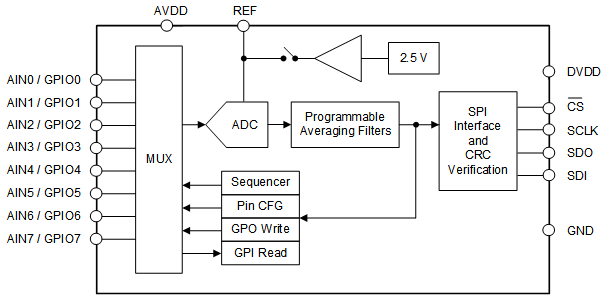
The ADS7066 features built-in offset calibration for improved accuracy over wide operating conditions of the system. The programmable averaging filters enable higher resolution measurement. The eight channels of the ADS7066 can be individually configured as analog inputs, digital inputs, or digital outputs that simplify circuit design for mixed signal feedback and digital control.

The enhanced-SPI enables the ADS7066 in achieving high throughput at lower clock speeds, thereby simplifying the board layout and lowering system cost. The ADS7066 features a cyclic redundancy check (CRC) for data read and write operations and the power-up configuration.

Package Information
PART NAME PACKAGE(1) PACKAGE SIZE (NOM)(2)
ADS7066 YBH (DSBGA, 16) 1.636 mm × 1.636 mm
RTE (WQFN, 16) 3.00 mm × 3.00 mm
For all available packages, see the orderable addendum at the end of the data sheet.
The package size (length × width) is a nominal value and includes pins, where applicable.
GUID-8EE0FA39-1EF5-4995-8937-AE1554F23EDC-low.gif ADS7066 Block Diagram