SBASA44B august 2021 – june 2023 AFE7900
PRODUCTION DATA
- 1
- 1Features
- 2Applications
- 3Description
- 4Revision History
-
5Specifications
- 5.1 Absolute Maximum Ratings
- 5.2 ESD Ratings
- 5.3 Recommended Operating Conditions
- 5.4 Thermal Information
- 5.5 Transmitter Electrical Characteristics
- 5.6 RF ADC Electrical Characteristics
- 5.7 PLL/VCO/Clock Electrical Characteristics
- 5.8 Digital Electrical Characteristics
- 5.9 Power Supply Electrical Characteristics
- 5.10 Timing Requirements
- 5.11 Switching Characteristics
- 5.12
Typical Characteristics
- 5.12.1 RX Typical Characteristics 30 MHz and 400 MHz
- 5.12.2 RX Typical Characteristics at 800MHz
- 5.12.3 RX Typical Characteristics 1.75GHz to 1.9GHz
- 5.12.4 RX Typical Characteristics 2.6GHz
- 5.12.5 RX Typical Characteristics 3.5GHz
- 5.12.6 RX Typical Characteristics 4.9GHz
- 5.12.7 TX Typical Characteristics at 30MHz and 400MHz
- 5.12.8 TX Typical Characteristics at 800MHz
- 5.12.9 TX Typical Characteristics at 1.8GHz
- 5.12.10 TX Typical Characteristics at 2.6GHz
- 5.12.11 TX Typical Characteristics at 3.5GHz
- 5.12.12 TX Typical Characteristics at 4.9GHz
- 5.12.13 TX Typical Characteristics at 7.1GHz
- 5.12.14 PLL and Clock Typical Characteristics
- 6Device and Documentation Support
- 7Mechanical, Packaging, and Orderable Information
Package Options
Mechanical Data (Package|Pins)
Thermal pad, mechanical data (Package|Pins)
Orderable Information
3 Description
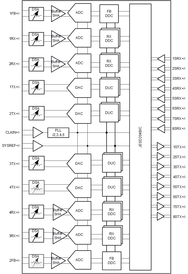
The AFE7900 is a high performance, wide bandwidth multi-channel transceiver, integrating four RF sampling transmitter chains, four RF sampling receiver chains and two RF sampling feedback chains (six RF sampling ADCs total). With operation up to 7.4 GHz, this device enables direct RF sampling in the L, S and C-band frequency ranges without the need for additional frequency conversions stages. This improvement in density and flexibility enables high-channel-count, multi-mission systems.
The TX signal paths support interpolation and digital up conversion options that deliver up to 1200 MHz of signal bandwidth for four TX or 2400 MHz for two TX. The output of the DUCs drives a 12-GSPS DAC (digital to analog converter) with a mixed mode output option to enhance 2nd Nyquist operation. The DAC output includes a variable gain amplifier (TX DSA) with 40-dB range and 1-dB analog and 0.125-dB digital steps.
Each receiver chain includes a 25-dB range DSA (Digital Step Attenuator), followed by a 3-GSPS ADC (analog-to-digital converter). Each receiver channel has an analog peak power detector and various digital power detectors to assist an external or internal autonomous automatic gain controller, and RF overload detectors for device reliability protection. Flexible decimation options provide optimization of data bandwidth up to 1200 MHz for four RX without FB paths or 600 MHz with two FB paths (1200 MHz BW each).
The device contains a SYSREF timing detector to allow optimization of the SYSREF input timing relative to the device clock.
 Functional Block Diagram