SPRS982H December 2016 – December 2019 AM5746 , AM5748 , AM5749
PRODUCTION DATA.
- 1Device Overview
- 2Revision History
- 3Device Comparison
-
4Terminal Configuration and Functions
- 4.1 Pin Diagram
- 4.2 Pin Attributes
- 4.3
Signal Descriptions
- 4.3.1 VIP
- 4.3.2 DSS
- 4.3.3 HDMI
- 4.3.4 EMIF
- 4.3.5 GPMC
- 4.3.6 Timer
- 4.3.7 I2C
- 4.3.8 HDQ1W
- 4.3.9 UART
- 4.3.10 McSPI
- 4.3.11 QSPI
- 4.3.12 McASP
- 4.3.13 USB
- 4.3.14 SATA
- 4.3.15 PCIe
- 4.3.16 DCAN and MCAN
- 4.3.17 GMAC_SW
- 4.3.18 MLB
- 4.3.19 eMMC/SD/SDIO
- 4.3.20 GPIO
- 4.3.21 KBD
- 4.3.22 PWM
- 4.3.23 PRU-ICSS
- 4.3.24 Test Interfaces
- 4.3.25 System and Miscellaneous
- 4.4 Pin Multiplexing
- 4.5 Connections for Unused Pins
-
5Specifications
- 5.1 Absolute Maximum Ratings
- 5.2 ESD Ratings
- 5.3 Power-On Hours (POH) Limits
- 5.4 Recommended Operating Conditions
- 5.5 Operating Performance Points
- 5.6 Power Consumption Summary
- 5.7
Electrical Characteristics
- Table 5-7 LVCMOS DDR DC Electrical Characteristics
- Table 5-8 Dual Voltage LVCMOS I2C DC Electrical Characteristics
- Table 5-9 IQ1833 Buffers DC Electrical Characteristics
- Table 5-10 IHHV1833 Buffers DC Electrical Characteristics
- Table 5-11 LVCMOS OSC Buffers DC Electrical Characteristics
- Table 5-12 BC1833IHHV Buffers DC Electrical Characteristics
- Table 5-13 Dual Voltage SDIO1833 DC Electrical Characteristics
- Table 5-14 Dual Voltage LVCMOS DC Electrical Characteristics
- 5.7.1 HDMIPHY DC Electrical Characteristics
- 5.7.2 USBPHY DC Electrical Characteristics
- 5.7.3 SATAPHY DC Electrical Characteristics
- 5.7.4 PCIEPHY DC Electrical Characteristics
- 5.8 VPP Specifications for One-Time Programmable (OTP) eFuses
- 5.9 Thermal Characteristics
- 5.10
Timing Requirements and Switching Characteristics
- 5.10.1 Timing Parameters and Information
- 5.10.2 Interface Clock Specifications
- 5.10.3 Power Supply Sequences
- 5.10.4 Clock Specifications
- 5.10.5 Recommended Clock and Control Signal Transition Behavior
- 5.10.6
Peripherals
- 5.10.6.1 Timing Test Conditions
- 5.10.6.2 Virtual and Manual I/O Timing Modes
- 5.10.6.3 VIP
- 5.10.6.4 DSS
- 5.10.6.5 HDMI
- 5.10.6.6 EMIF
- 5.10.6.7 GPMC
- 5.10.6.8 I2C
- 5.10.6.9 HDQ1W
- 5.10.6.10 UART
- 5.10.6.11 McSPI
- 5.10.6.12 QSPI
- 5.10.6.13
McASP
- Table 5-80 Timing Requirements for McASP1
- Table 5-81 Timing Requirements for McASP2
- Table 5-82 Timing Requirements for McASP3/4/5/6/7/8
- Table 5-83 Switching Characteristics Over Recommended Operating Conditions for McASP1
- Table 5-84 Switching Characteristics Over Recommended Operating Conditions for McASP2
- Table 5-85 Switching Characteristics Over Recommended Operating Conditions for McASP3/4/5/6/7/8
- 5.10.6.14 USB
- 5.10.6.15 SATA
- 5.10.6.16 PCIe
- 5.10.6.17 CAN
- 5.10.6.18
GMAC_SW
- 5.10.6.18.1
GMAC MII Timings
- Table 5-99 Timing Requirements for miin_rxclk - MII Operation
- Table 5-100 Timing Requirements for miin_txclk - MII Operation
- Table 5-101 Timing Requirements for GMAC MIIn Receive 10/100 Mbit/s
- Table 5-102 Switching Characteristics Over Recommended Operating Conditions for GMAC MIIn Transmit 10/100 Mbits/s
- 5.10.6.18.2 GMAC MDIO Interface Timings
- 5.10.6.18.3
GMAC RMII Timings
- Table 5-107 Timing Requirements for GMAC REF_CLK - RMII Operation
- Table 5-108 Timing Requirements for GMAC RMIIn Receive
- Table 5-109 Switching Characteristics Over Recommended Operating Conditions for GMAC REF_CLK - RMII Operation
- Table 5-110 Switching Characteristics Over Recommended Operating Conditions for GMAC RMIIn Transmit 10/100 Mbits/s
- 5.10.6.18.4
GMAC RGMII Timings
- Table 5-114 Timing Requirements for rgmiin_rxc - RGMIIn Operation
- Table 5-115 Timing Requirements for GMAC RGMIIn Input Receive for 10/100/1000 Mbps
- Table 5-116 Switching Characteristics Over Recommended Operating Conditions for rgmiin_txctl - RGMIIn Operation for 10/100/1000 Mbit/s
- Table 5-117 Switching Characteristics for GMAC RGMIIn Output Transmit for 10/100/1000 Mbps
- 5.10.6.18.1
GMAC MII Timings
- 5.10.6.19
eMMC/SD/SDIO
- 5.10.6.19.1
MMC1—SD Card Interface
- 5.10.6.19.1.1 Default speed, 4-bit data, SDR, half-cycle
- 5.10.6.19.1.2 High speed, 4-bit data, SDR, half-cycle
- 5.10.6.19.1.3 SDR12, 4-bit data, half-cycle
- 5.10.6.19.1.4 SDR25, 4-bit data, half-cycle
- 5.10.6.19.1.5 UHS-I SDR50, 4-bit data, half-cycle
- 5.10.6.19.1.6 UHS-I SDR104, 4-bit data, half-cycle
- 5.10.6.19.1.7 UHS-I DDR50, 4-bit data
- 5.10.6.19.2 MMC2 — eMMC
- 5.10.6.19.3 MMC3 and MMC4—SDIO/SD
- 5.10.6.19.1
MMC1—SD Card Interface
- 5.10.6.20
PRU-ICSS
- 5.10.6.20.1 Programmable Real-Time Unit (PRU-ICSS PRU)
- 5.10.6.20.2
PRU-ICSS EtherCAT (PRU-ICSS ECAT)
- 5.10.6.20.2.1
PRU-ICSS ECAT Electrical Data and Timing
- Table 5-174 PRU-ICSS ECAT Timing Requirements – Input Validated With LATCH_IN
- Table 5-175 PRU-ICSS ECAT Timing Requirements – Input Validated With SYNCx
- Table 5-176 PRU-ICSS ECAT Timing Requirements – Input Validated With Start of Frame (SOF)
- Table 5-177 PRU-ICSS ECAT Timing Requirements - LATCHx_IN
- Table 5-178 PRU-ICSS ECAT Switching Requirements - Digital IOs
- 5.10.6.20.2.1
PRU-ICSS ECAT Electrical Data and Timing
- 5.10.6.20.3 PRU-ICSS MII_RT and Switch
- 5.10.6.20.4 PRU-ICSS Universal Asynchronous Receiver Transmitter (PRU-ICSS UART)
- 5.10.6.20.5 PRU-ICSS IOSETs
- 5.10.6.20.6 PRU-ICSS Manual Functional Mapping
- 5.10.6.21 System and Miscellaneous interfaces
- 5.10.7
Emulation and Debug Subsystem
- 5.10.7.1
JTAG
- 5.10.7.1.1
JTAG Electrical Data/Timing
- Table 5-210 Timing Requirements for IEEE 1149.1 JTAG
- Table 5-211 Switching Characteristics Over Recommended Operating Conditions for IEEE 1149.1 JTAG
- Table 5-212 Timing Requirements for IEEE 1149.1 JTAG With RTCK
- Table 5-213 Switching Characteristics Over Recommended Operating Conditions for IEEE 1149.1 JTAG With RTCK
- 5.10.7.1.1
JTAG Electrical Data/Timing
- 5.10.7.2 TPIU
- 5.10.7.1
JTAG
-
6Detailed Description
- 6.1 Overview
- 6.2 Processor Subsystems
- 6.3 Accelerators and Coprocessors
- 6.4
Other Subsystems
- 6.4.1 Memory Subsystem
- 6.4.2 EDMA
- 6.4.3 Peripherals
- 6.4.4 On-Chip Debug
- 6.5 Identification
- 6.6 Boot Modes
-
7Applications, Implementation, and Layout
- 7.1 Power Supply Mapping
- 7.2
DDR3 Board Design and Layout Guidelines
- 7.2.1 DDR3 General Board Layout Guidelines
- 7.2.2
DDR3 Board Design and Layout Guidelines
- 7.2.2.1 Board Designs
- 7.2.2.2 DDR3 EMIFs
- 7.2.2.3 DDR3 Device Combinations
- 7.2.2.4 DDR3 Interface Schematic
- 7.2.2.5 Compatible JEDEC DDR3 Devices
- 7.2.2.6 PCB Stackup
- 7.2.2.7 Placement
- 7.2.2.8 DDR3 Keepout Region
- 7.2.2.9 Bulk Bypass Capacitors
- 7.2.2.10 High Speed Bypass Capacitors
- 7.2.2.11 Net Classes
- 7.2.2.12 DDR3 Signal Termination
- 7.2.2.13 VREF_DDR Routing
- 7.2.2.14 VTT
- 7.2.2.15 CK and ADDR_CTRL Topologies and Routing Definition
- 7.2.2.16 Data Topologies and Routing Definition
- 7.2.2.17 Routing Specification
- 7.3 High Speed Differential Signal Routing Guidance
- 7.4 Power Distribution Network Implementation Guidance
- 7.5 Thermal Solution Guidance
- 7.6 Single-Ended Interfaces
- 7.7 LJCB_REFN/P Connections
- 7.8 Clock Routing Guidelines
- 8Device and Documentation Support
- 9Mechanical, Packaging, and Orderable Information
Package Options
Refer to the PDF data sheet for device specific package drawings
Mechanical Data (Package|Pins)
- ABZ|760
Thermal pad, mechanical data (Package|Pins)
Orderable Information
5.10.6.11 McSPI
The McSPI is a master/slave synchronous serial bus. There are four separate McSPI modules (SPI1, SPI2, SPI3, and SPI4) in the device. All these four modules support up to four external devices (four chip selects) and are able to work as both master and slave.
The McSPI modules include the following main features:
- Serial clock with programmable frequency, polarity, and phase for each channel
- Wide selection of SPI word lengths, ranging from 4 to 32 bits
- Up to four master channels, or single channel in slave mode
- Master multichannel mode:
- Full duplex/half duplex
- Transmit-only/receive-only/transmit-and-receive modes
- Flexible input/output (I/O) port controls per channel
- Programmable clock granularity
- SPI configuration per channel. This means, clock definition, polarity enabling and word width
- Power management through wake-up capabilities
- Programmable timing control between chip select and external clock generation
- Built-in FIFO available for a single channel.
- Each SPI module supports multiple chip select pins spim_cs[i], where i = 1 to 4.
NOTE
For more information, see Serial Communication Interface section in the device TRM.
NOTE
The McSPIm module (m = 1 to 4) is also referred to as SPIm.
CAUTION
The IO timings provided in this section are applicable for all combinations of signals for SPI1 and SPI2. However, the timings are only valid for SPI3 and SPI4 if signals within a single IOSET are used. The IOSETS are defined in the Table 5-76.
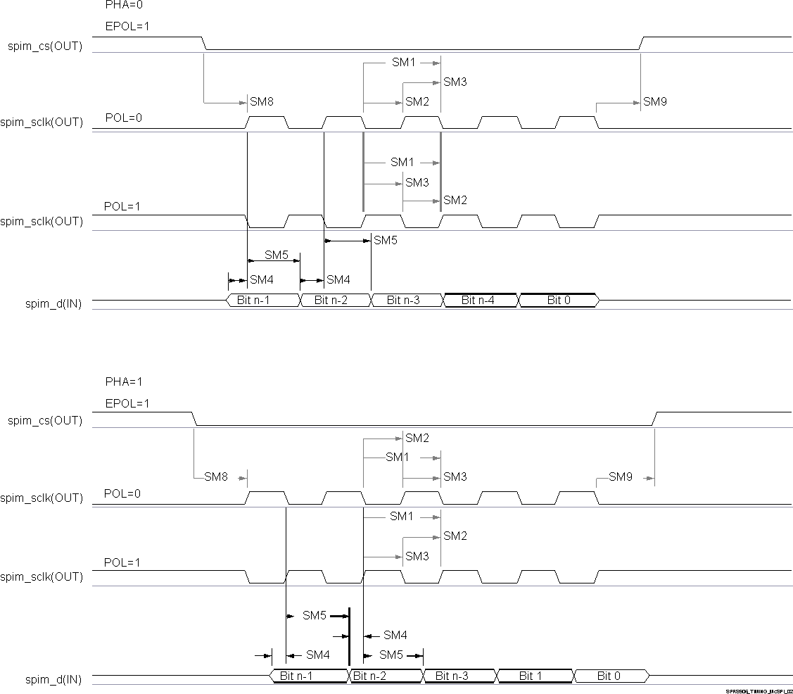
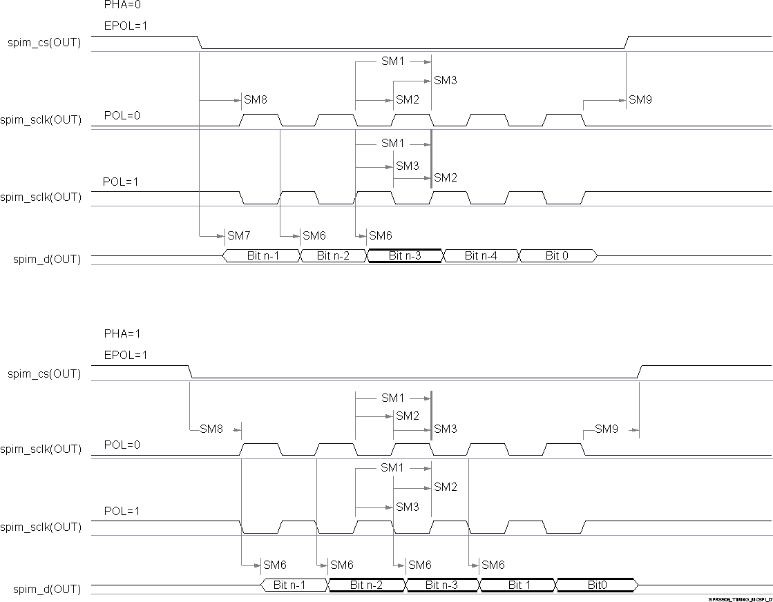
Table 5-74, Figure 5-50 and Figure 5-51 present timing requirements for McSPI - master mode.
Table 5-74 Timing Requirements for SPI - Master Mode (1)(8)
| NO. | PARAMETER | DESCRIPTION | MODE | MIN | MAX | UNIT |
|---|---|---|---|---|---|---|
| SM1 | tc(SPICLK) | Cycle time, spi_sclk (1)(2) | SPI1/2/3/4 | 20.8 (3) | ns | |
| SM2 | tw(SPICLKL) | Typical Pulse duration, spi_sclk low (1) | 0.5*P-1 (4) | ns | ||
| SM3 | tw(SPICLKH) | Typical Pulse duration, spi_sclk high (1) | 0.5*P-1 (4) | ns | ||
| SM4 | tsu(MISO-SPICLK) | Setup time, spi_d[x] valid before spi_sclk active edge (1) | 4.4 | ns | ||
| SM5 | th(SPICLK-MISO) | Hold time, spi_d[x] valid after spi_sclk active edge (1) | 3.9 | ns | ||
| SM6 | td(SPICLK-SIMO) | Delay time, spi_sclk active edge to spi_d[x] transition (1) | SPI1 | -4.27 | 4.27 | ns |
| SPI2 | -4.32 | 4.32 | ns | |||
| SPI3 | -5.37 | 4.23 | ns | |||
| SPI4 | -3.81 | 4.41 | ns | |||
| SM7 | td(CS-SIMO) | Delay time, spi_cs[x] active edge to spi_d[x] transition | 5 | ns | ||
| SM8 | td(CS-SPICLK) | Delay time, spi_cs[x] active to spi_sclk first edge (1) | MASTER_PHA0 (5) | B-4.6 (6) | ns | |
| MASTER_PHA1 (5) | A-4.6 (7) | ns | ||||
| SM9 | td(SPICLK-CS) | Delay time, spi_sclk last edge to spi_cs[x] inactive (1) | MASTER_PHA0 (5) | A-4.6 (7) | ns | |
| MASTER_PHA1 (5) | B-4.6 (6) | ns |
- This timing applies to all configurations regardless of SPI_CLK polarity and which clock edges are used to drive output data and capture input data.
- Related to the SPI_CLK maximum frequency.
- 20.8 ns cycle time = 48 MHz
- P = SPICLK period.
- SPI_CLK phase is programmable with the PHA bit of the SPI_CH(i)CONF register.
- B = (TCS + 0.5) × TSPICLKREF × Fratio, where TCS is a bit field of the SPI_CH(i)CONF register and Fratio = Even ≥ 2.
- When P = 20.8 ns, A = (TCS + 1) × TSPICLKREF, where TCS is a bit field of the SPI_CH(i)CONF register. When P > 20.8 ns, A = (TCS + 0.5) × Fratio × TSPICLKREF, where TCS is a bit field of the SPI_CH(i)CONF register.
- The IO timings provided in this section are applicable for all combinations of signals for SPI1 and SPI2. However, the timings are only valid for SPI3 and SPI4 if signals within a single IOSET are used. The IOSETs are defined in the following tables.
 Figure 5-51 McSPI - Master Mode Receive
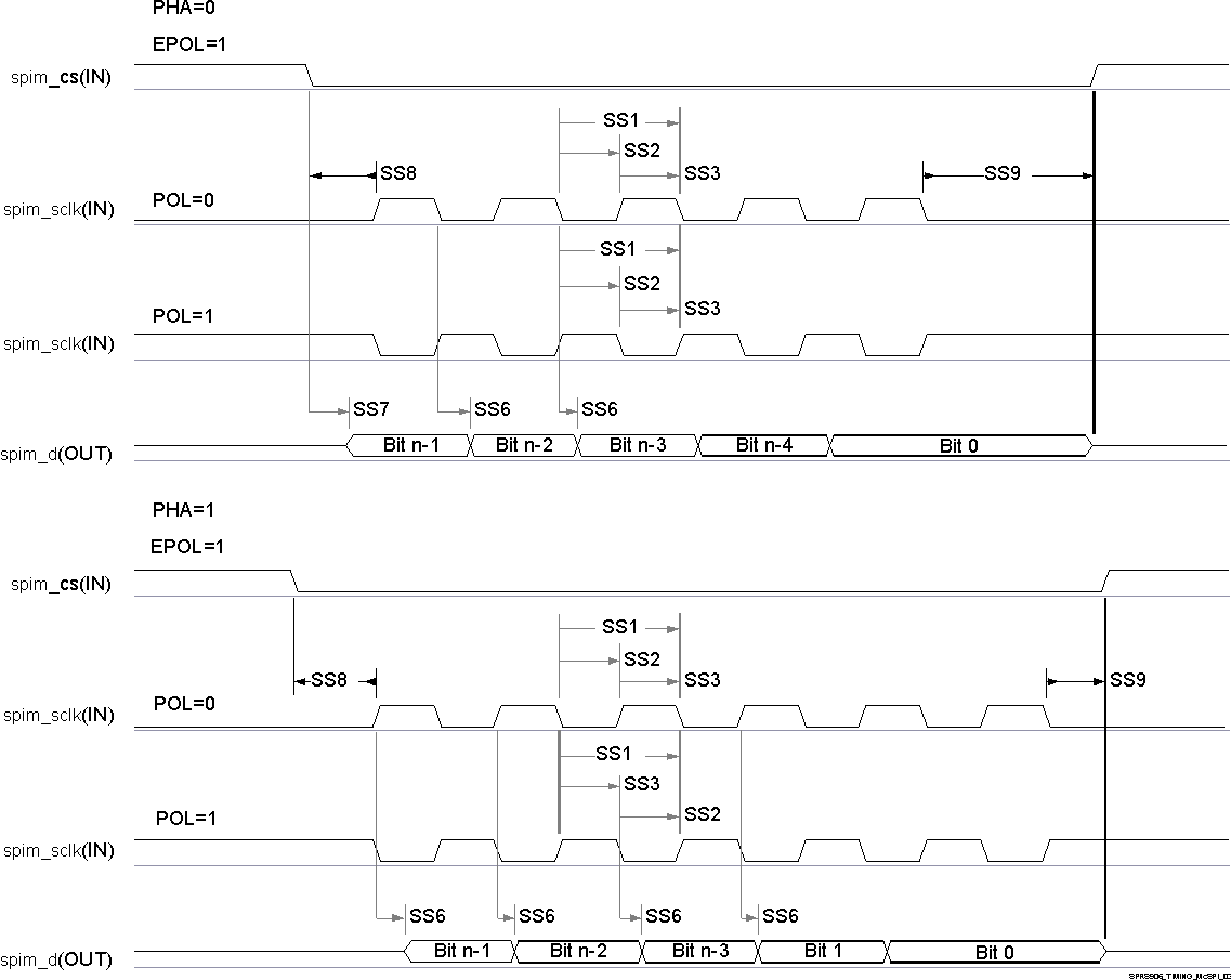
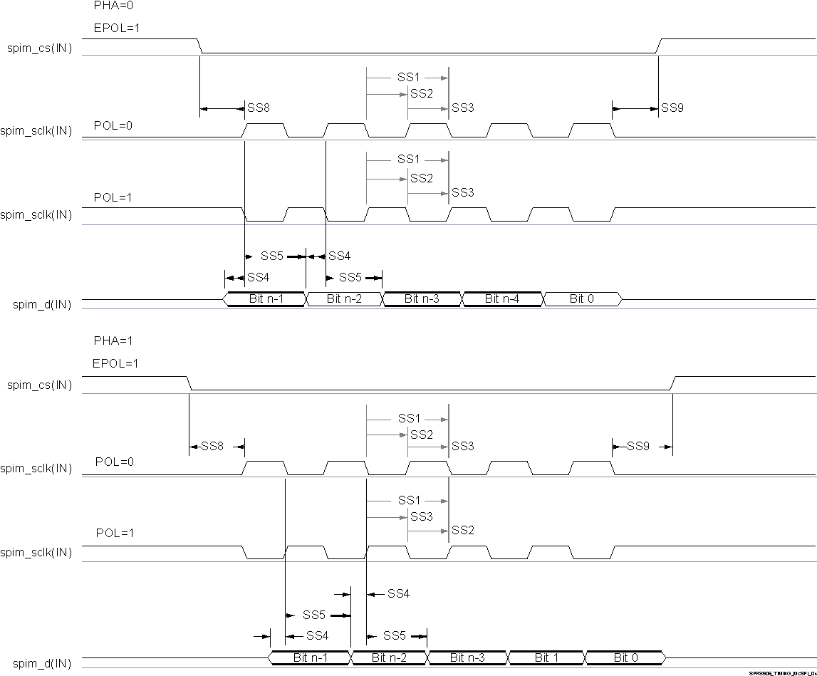
 Table 5-75, Figure 5-52 and Figure 5-53 present timing requirements for McSPI - slave mode.
Table 5-75 Timing Requirements for SPI - Slave Mode(6)
| NO. | PARAMETER | DESCRIPTION | MODE | MIN | MAX | UNIT |
|---|---|---|---|---|---|---|
| SS1(2)(1) | tc(SPICLK) | Cycle time, spi_sclk (3) | 62.5 | ns | ||
| SS2(1) | tw(SPICLKL) | Typical Pulse duration, spi_sclk low | 0.45P (4) | ns | ||
| SS3(1) | tw(SPICLKH) | Typical Pulse duration, spi_sclk high | 0.45P (4) | ns | ||
| SS4(1) | tsu(SIMO-SPICLK) | Setup time, spi_d[x] valid before spi_sclk active edge | 5 | ns | ||
| SS5(1) | th(SPICLK-SIMO) | Hold time, spi_d[x] valid after spi_sclk active edge | 5 | ns | ||
| SS6(1) | td(SPICLK-SOMI) | Delay time, spi_sclk active edge to mcspi_somi transition | SPI1/2/3 | 2 | 26.1 | ns |
| SPI4 | 2 | 18 | ns | |||
| SS7(5) | td(CS-SOMI) | Delay time, spi_cs[x] active edge to mcspi_somi transition | 20.95 | ns | ||
| SS8(1) | tsu(CS-SPICLK) | Setup time, spi_cs[x] valid before spi_sclk first edge | 5 | ns | ||
| SS9(1) | th(SPICLK-CS) | Hold time, spi_cs[x] valid after spi_sclk last edge | 5 | ns |
- This timing applies to all configurations regardless of SPI_CLK polarity and which clock edges are used to drive output data and capture input data.
- When operating the SPI interface in RX-only mode, the minimum Cycle time is 26 ns (38.4 MHz)
- 62.5 ns Cycle time = 16 MHz
- P = SPICLK period.
- PHA = 0; SPI_CLK phase is programmable with the PHA bit of the SPI_CH(i)CONF register.
- The IO timings provided in this section are applicable for all combinations of signals for SPI1 and SPI2. However, the timings are only valid for SPI3 and SPI4 if signals within a single IOSET are used. The IOSETs are defined in the following tables.
 Figure 5-52 McSPI - Slave Mode Transmit
  Figure 5-53 McSPI - Slave Mode Receive
 In Table 5-76 are presented the specific groupings of signals (IOSET) for use with SPI3 and SPI4.
Table 5-76 McSPI3/4 IOSETs
| Signal | IOSET1 | IOSET2 | IOSET3 | IOSET4 | IOSET5 | IOSET6 | ||||||
|---|---|---|---|---|---|---|---|---|---|---|---|---|
| BALL | MUX | BALL | MUX | BALL | MUX | BALL | MUX | BALL | MUX | BALL | MUX | |
| SPI3 | ||||||||||||
| spi3_sclk | AD9 | 8 | E11 | 8 | V2 | 7 | B12 | 3 | C18 | 2 | AC4 | 1 |
| spi3_d1 | AF9 | 8 | B10 | 8 | Y1 | 7 | A11 | 3 | A21 | 2 | AC7 | 1 |
| spi3_d0 | AE9 | 8 | C11 | 8 | W9 | 7 | B13 | 3 | G16 | 2 | AC6 | 1 |
| spi3_cs0 | AF8 | 8 | D11 | 8 | V9 | 7 | A12 | 3 | D17 | 2 | AC9 | 1 |
| spi3_cs1 | AC3 | 1 | B11 | 8 | AC3 | 1 | E14 | 3 | B11 | 8 | AC3 | 1 |
| spi3_cs2 | - | - | F11 | 8 | - | - | F11 | 8 | F11 | 8 | - | - |
| spi3_cs3 | - | - | A10 | 8 | - | - | A10 | 8 | A10 | 8 | - | - |
| SPI4 | ||||||||||||
| spi4_sclk | N7 | 8 | G1 | 8 | V7 | 7 | AA3 | 2 | AC8 | 1 | - | - |
| spi4_d1 | R4 | 8 | G6 | 8 | U7 | 7 | AB9 | 2 | AD6 | 1 | - | - |
| spi4_d0 | N9 | 8 | F2 | 8 | V6 | 7 | AB3 | 2 | AB8 | 1 | - | - |
| spi4_cs0 | P9 | 8 | F3 | 8 | U6 | 7 | AA4 | 2 | AB5 | 1 | - | - |
| spi4_cs1 | P4 | 8 | P4 | 8 | Y1 | 8 | Y1 | 8 | Y1 | 8 | - | - |
| spi4_cs2 | R3 | 8 | R3 | 8 | W9 | 8 | W9 | 8 | W9 | 8 | - | - |
| spi4_cs3 | T2 | 8 | T2 | 8 | V9 | 8 | V9 | 8 | V9 | 8 | - | - |
