SLUS892D December 2009 – December 2019 BQ24610 , BQ24617
PRODUCTION DATA.
- 1 Features
- 2 Applications
- 3 Description
- 4 Revision History
- 5 Description (continued)
- 6 Device Comparison Table
- 7 Pin Configuration and Functions
- 8 Specifications
-
9 Detailed Description
- 9.1 Overview
- 9.2 Functional Block Diagram
- 9.3
Feature Description
- 9.3.1 Battery Voltage Regulation
- 9.3.2 Battery Current Regulation
- 9.3.3 Input Adapter Current Regulation
- 9.3.4 Precharge
- 9.3.5 Charge Termination, Recharge, and Safety Timer
- 9.3.6 Power Up
- 9.3.7 Enable and Disable Charging
- 9.3.8 System Power Selector
- 9.3.9 Automatic Internal Soft-Start Charger Current
- 9.3.10 Converter Operation
- 9.3.11 Synchronous and Nonsynchronous Operation
- 9.3.12 Cycle-by-Cycle Charge Undercurrent Protection
- 9.3.13 Input Overvoltage Protection (ACOV)
- 9.3.14 Input Undervoltage Lockout (UVLO)
- 9.3.15 Battery Overvoltage Protection
- 9.3.16 Cycle-by-Cycle Charge Overcurrent Protection
- 9.3.17 Thermal Shutdown Protection
- 9.3.18 Temperature Qualification
- 9.3.19 Timer Fault Recovery
- 9.3.20 PG Output
- 9.3.21 CE (Charge Enable)
- 9.3.22 Charge Status Outputs
- 9.3.23 Battery Detection
- 9.4 Device Functional Modes
- 10Application and Implementation
- 11Power Supply Recommendations
- 12Layout
- 13Device and Documentation Support
- 14Mechanical, Packaging, and Orderable Information
Package Options
Mechanical Data (Package|Pins)
- RGE|24
Thermal pad, mechanical data (Package|Pins)
- RGE|24
Orderable Information
10.2.1.2.5 Input Filter Design
During adapter hot plug-in, the parasitic inductance and input capacitor from the adapter cable form a second-order system. The voltage spike at the VCC pin may be beyond the IC maximum voltage rating and damage the IC. The input filter must be carefully designed and tested to prevent an overvoltage event on the VCC pin. The ACP/ACN pins must be placed after the input ACFET in order to avoid overvoltage stress on these pins during hot plug-in.
There are several methods for damping or limiting the overvoltage spike during adapter hot plug-in. An electrolytic capacitor with high ESR as an input capacitor can damp the overvoltage spike well below the IC maximum pin voltage rating. A high-current capability TVS Zener diode can also limit the overvoltage level to an IC safe level. However these two solutions may not have low cost or small size.
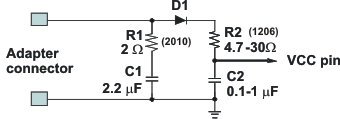
A cost-effective and small size-solution is shown in Figure 21. The R1 and C1 are composed of a damping RC network to damp the hot plug-in oscillation. As a result, the overvoltage spike is limited to a safe level. D1 is used for reverse voltage protection for the VCC pin (it can be the body diode of input ACFET). C2 is VCC pin decoupling capacitor and it should be placed as close as possible to the VCC pin. R2 and C2 form a damping RC network to further protect the IC from high dv/dt and high-voltage spike. The C2 value should be less than the C1 value so R1 can be dominant over the ESR of C1 to get enough damping effect for hot plug-in. The R1 and R2 packages must be sized to handle in-rush current power loss according to resistor manufacturer’s datasheet. The filter component values always must be verified with the real application and minor adjustments may be needed to fit in the real application circuit.
 Figure 21. Input Filter