SLUS892D December 2009 – December 2019 BQ24610 , BQ24617
PRODUCTION DATA.
- 1 Features
- 2 Applications
- 3 Description
- 4 Revision History
- 5 Description (continued)
- 6 Device Comparison Table
- 7 Pin Configuration and Functions
- 8 Specifications
-
9 Detailed Description
- 9.1 Overview
- 9.2 Functional Block Diagram
- 9.3
Feature Description
- 9.3.1 Battery Voltage Regulation
- 9.3.2 Battery Current Regulation
- 9.3.3 Input Adapter Current Regulation
- 9.3.4 Precharge
- 9.3.5 Charge Termination, Recharge, and Safety Timer
- 9.3.6 Power Up
- 9.3.7 Enable and Disable Charging
- 9.3.8 System Power Selector
- 9.3.9 Automatic Internal Soft-Start Charger Current
- 9.3.10 Converter Operation
- 9.3.11 Synchronous and Nonsynchronous Operation
- 9.3.12 Cycle-by-Cycle Charge Undercurrent Protection
- 9.3.13 Input Overvoltage Protection (ACOV)
- 9.3.14 Input Undervoltage Lockout (UVLO)
- 9.3.15 Battery Overvoltage Protection
- 9.3.16 Cycle-by-Cycle Charge Overcurrent Protection
- 9.3.17 Thermal Shutdown Protection
- 9.3.18 Temperature Qualification
- 9.3.19 Timer Fault Recovery
- 9.3.20 PG Output
- 9.3.21 CE (Charge Enable)
- 9.3.22 Charge Status Outputs
- 9.3.23 Battery Detection
- 9.4 Device Functional Modes
- 10Application and Implementation
- 11Power Supply Recommendations
- 12Layout
- 13Device and Documentation Support
- 14Mechanical, Packaging, and Orderable Information
Package Options
Mechanical Data (Package|Pins)
- RGE|24
Thermal pad, mechanical data (Package|Pins)
- RGE|24
Orderable Information
10.2.1 System with Power Path
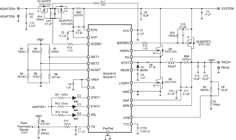
BQ24610 can be configured for Power Path applications, where input source can be used to power both system as well as charge the battery. If input source is removed, then battery is automatically connected to the system. Figure 20 shows typical schematic when using BQ24610 with Power Path, input current regulation and input reverse protection FET.

VIN = 19 V, 3-cell, Iadapter_limit = 4 A, Icharge = 3 A, Ipre-charge = Iterm = 0.3 A, 5-hour saftey timer
Figure 20. System Schematic with Power Path