SLUSF18A October   2023  – December 2023 BQ25638

PRODUCTION DATA  

  1.   1
  2. Features
  3. Applications
  4. Description
  5. Description (continued)
  6. Pin Configuration and Functions
  7. Specifications
    1. 6.1 Absolute Maximum Ratings
    2. 6.2 ESD Ratings
    3. 6.3 Recommended Operating Conditions
    4. 6.4 Thermal Information
    5. 6.5 Electrical Characteristics
    6. 6.6 Timing Requirements
    7. 6.7 Typical Characteristics
  8. Detailed Description
    1. 7.1 Overview
    2. 7.2 Functional Block Diagram
    3. 7.3 Feature Description
      1. 7.3.1  Power-On-Reset (POR)
      2. 7.3.2  Device Power Up from Battery
      3. 7.3.3  Device Power Up from Input Source
        1. 7.3.3.1 REGN LDO Power Up
        2. 7.3.3.2 Poor Source Qualification
        3. 7.3.3.3 Input Voltage Limit Threshold Setting (VINDPM Threshold)
        4. 7.3.3.4 Converter Power-Up
        5. 7.3.3.5 Input Current Optimizer (ICO)
        6. 7.3.3.6 Switching Frequency and Dithering Feature
      4. 7.3.4  Power Path Management
        1. 7.3.4.1 Narrow VDC Architecture
        2. 7.3.4.2 Dynamic Power Management
          1. 7.3.4.2.1 Input Current Limit on ILIM Pin
        3. 7.3.4.3 High Impedance (HIZ) Mode
      5. 7.3.5  Battery Charging Management
        1. 7.3.5.1 Autonomous Charging Cycle
        2. 7.3.5.2 Battery Charging Profile
        3. 7.3.5.3 Charging Termination
        4. 7.3.5.4 Thermistor Qualification
          1. 7.3.5.4.1 Advanced Temperature Profile in Charge Mode
          2. 7.3.5.4.2 TS Pin Thermistor Configuration
          3. 7.3.5.4.3 Cold/Hot Temperature Window in OTG Mode
          4. 7.3.5.4.4 JEITA Charge Rate Scaling
          5. 7.3.5.4.5 TS_BIAS Pin
        5. 7.3.5.5 Charging Safety Timers
      6. 7.3.6  USB On-The-Go (OTG)
        1. 7.3.6.1 Boost OTG Mode
      7. 7.3.7  Integrated 12-bit ADC for Monitoring
      8. 7.3.8  Status Outputs (INT , PG , STAT)
        1. 7.3.8.1 PG Pin Power Good Indicator
        2. 7.3.8.2 Charging Status Indicator (STAT)
        3. 7.3.8.3 Interrupt to Host (INT)
      9. 7.3.9  BATFET Control
        1. 7.3.9.1 Shutdown Mode
        2. 7.3.9.2 Ultra-Low Power Mode
        3. 7.3.9.3 System Power Reset
      10. 7.3.10 Protections
        1. 7.3.10.1 Voltage and Current Monitoring in Battery Only and HIZ Modes
          1. 7.3.10.1.1 Battery Overcurrent Protection
          2. 7.3.10.1.2 Battery Undervoltage Lockout
        2. 7.3.10.2 Voltage and Current Monitoring in Forward Mode
          1. 7.3.10.2.1 Input Overvoltage
          2. 7.3.10.2.2 System Overvoltage Protection (SYSOVP)
          3. 7.3.10.2.3 Forward Converter Cycle-by-Cycle Current Limit
          4. 7.3.10.2.4 System Short
          5. 7.3.10.2.5 Battery Overvoltage Protection (BATOVP)
          6. 7.3.10.2.6 Sleep and Poor Source Comparators
        3. 7.3.10.3 Voltage and Current Monitoring in Reverse Mode
          1. 7.3.10.3.1 Boost Mode Overvoltage Protection
          2. 7.3.10.3.2 Boost Mode Duty Cycle Protection
          3. 7.3.10.3.3 Boost Mode PMID Undervoltage Protection
          4. 7.3.10.3.4 Boost Mode Battery Undervoltage
          5. 7.3.10.3.5 Boost Converter Cycle-by-Cycle Current Limit
          6. 7.3.10.3.6 Boost Mode SYS Short
        4. 7.3.10.4 Thermal Regulation and Thermal Shutdown
          1. 7.3.10.4.1 Thermal Protection in Buck Mode
          2. 7.3.10.4.2 Thermal Protection in Boost Mode
          3. 7.3.10.4.3 Thermal Protection in Battery-only Mode
    4. 7.4 Device Functional Modes
      1. 7.4.1 Host Mode and Default Mode
      2. 7.4.2 Register Bit Reset
    5. 7.5 Programming
      1. 7.5.1 Serial Interface
        1. 7.5.1.1 Data Validity
        2. 7.5.1.2 START and STOP Conditions
        3. 7.5.1.3 Byte Format
        4. 7.5.1.4 Acknowledge (ACK) and Not Acknowledge (NACK)
        5. 7.5.1.5 Target Address and Data Direction Bit
        6. 7.5.1.6 Single Write and Read
        7. 7.5.1.7 Multi-Write and Multi-Read
    6. 7.6 BQ25638 Registers
  9. Application and Implementation
    1. 8.1 Application Information
    2. 8.2 Typical Application
      1. 8.2.1 Design Requirements
      2. 8.2.2 Detailed Design Procedure
        1. 8.2.2.1 Inductor Selection
        2. 8.2.2.2 Input Capacitor
        3. 8.2.2.3 Output Capacitor
      3. 8.2.3 Application Curves
  10. Power Supply Recommendations
  11. 10Layout
    1. 10.1 Layout Guidelines
    2. 10.2 Layout Example
  12. 11Device and Documentation Support
    1. 11.1 Device Support
      1. 11.1.1 Third-Party Products Disclaimer
    2. 11.2 Documentation Support
      1. 11.2.1 Related Documentation
    3. 11.3 Receiving Notification of Documentation Updates
    4. 11.4 Support Resources
    5. 11.5 Trademarks
    6. 11.6 Electrostatic Discharge Caution
    7. 11.7 Glossary
  13. 12Revision History
  14. 13Mechanical, Packaging, and Orderable Information

Package Options

Refer to the PDF data sheet for device specific package drawings

Mechanical Data (Package|Pins)
  • YBG|30
Thermal pad, mechanical data (Package|Pins)
Orderable Information
TS Pin Thermistor Configuration

The typical TS resistor network is illustrated below.

GUID-79DA6DA4-6A5A-47EF-BBAD-627A48D5EE2D-low.svgFigure 7-5 TS Resistor Network

The value of RT1 and RT2 are determined from the resistance of the recommended 103AT-2 thermistor at 0ºC and 60 ºC (RTH0ºC= 27.28 kΩ and RTH60ºC = 3.02 kΩ) and the corresponding voltage thresholds VTS_COLD and VTS_HOT (expressed as percentage of REGN with value between 0 and 1).

Equation 3. RT2 = RTH 0ºC × RTH 60ºC × ( 1 V TS_0ºC - 1 V TS_60ºC ) RTH 60ºC × ( 1 V TS_60ºC - 1 ) - RTH 0ºC × ( 1 V TS_0ºC - 1 )
Equation 4. RT1 = 1 V TS_0ºC - 1 1 R T2 + 1 RTH 0ºC
Equation 5. GUID-6D3D84FE-8103-4DFB-868A-9541B64E767E-low.gif
Equation 6. GUID-91B435A0-F3A0-4B67-AFAE-3D47DB756464-low.gif

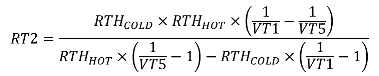
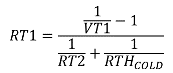
Assuming a 103AT-2 NTC thermistor on the battery pack, the RT1 and RT2 are calculated to be 5.24 kΩ and 30.31 kΩ respectively.

If the thermistor is biased from TS_BIAS, the maximum current should be checked against ITS_BIAS_FAULT. For the worst-case condition of thermistor at 0 Ω impedance (very hot), the bias current is:

Equation 7. I BIAS_MAX = V REGN RT1

For 5.30 kΩ RT1, this has a maximum IBIAS of 0.94 mA, which is well below the minimum ITS_BIAS_FAULT threshold. The 103AT-2 NTC thermistor is the recommended thermistor and has 10 kΩ nominal impedance. Using a lower impedance thermistor will change the value of R1 and may produce a bias current that exceeds the TS_BIAS pin fault threshold. TS_STAT[2:0] is set to 111.