SLVSDU0B September 2017 – September 2019 BQ25910
PRODUCTION DATA.
- 1 Features
- 2 Applications
- 3 Description
- 4 Revision History
- 5 Pin Configuration and Functions
- 6 Specifications
-
7 Detailed Description
- 7.1 Overview
- 7.2 Functional Block Diagram
- 7.3
Feature Description
- 7.3.1 Device Power-On-Reset (POR)
- 7.3.2 Device Power Up from Battery without Input Source
- 7.3.3 Device Power Up from Input Source
- 7.3.4 Power Up REGN LDO
- 7.3.5 Poor Source Qualification
- 7.3.6 Converter Power-Up
- 7.3.7 Three-Level Buck Converter Theory of Operation
- 7.3.8 Host Mode and Default Mode
- 7.3.9 Battery Charging Management
- 7.3.10 Master Charger and Parallel Charger Interactions
- 7.3.11 Battery Charging Profile
- 7.4 Device Functional Modes
- 7.5 Programming
- 7.6
Register Maps
- 7.6.1
I2C Registers
- 7.6.1.1 Battery Voltage Regulation Limit Register (Address = 0h) [reset = AAh]
- 7.6.1.2 Charger Current Limit Register (Address = 1h) [reset = 46h]
- 7.6.1.3 Input Voltage Limit Register (Address = 2h) [reset = 04h]
- 7.6.1.4 Input Current Limit Register (Address = 3h) [reset = 13h]
- 7.6.1.5 Reserved Register (Address = 4h) [reset = 03h]
- 7.6.1.6 Charger Control 1 Register (Address = 5h) [reset = 9Dh]
- 7.6.1.7 Charger Control 2 Register (Address = 6h) [reset = 33h]
- 7.6.1.8 INT Status Register (Address = 7h) [reset = X]
- 7.6.1.9 FAULT Status Register (Address = 8h) [reset = X]
- 7.6.1.10 INT Flag Status Register (Address = 9h) [reset = 00h]
- 7.6.1.11 FAULT Flag Register (Address = Ah) [reset = 00h]
- 7.6.1.12 INT Mask Register (Address = Bh) [reset = 00h]
- 7.6.1.13 FAULT Mask Register (Address = Ch) [reset = 00h]
- 7.6.1.14 Part Information Register (Address = Dh) [reset = 0Ah]
- 7.6.1
I2C Registers
- 8 Application and Implementation
- 9 Power Supply Recommendations
- 10Layout
- 11Device and Documentation Support
- 12Mechanical, Packaging, and Orderable Information
Package Options
Refer to the PDF data sheet for device specific package drawings
Mechanical Data (Package|Pins)
- YFF|36
Thermal pad, mechanical data (Package|Pins)
Orderable Information
7.4.3 Interrupt to Host (INT)
In some applications, the host does not always monitor the charger operation. The INT pin notifies the system host on the device operation. By default, the following events will generate an active-low, 256-μs INT pulse.
- Good input source detected (three conditions below met)
- VVBUS > VBAT (not in sleep)
- VVBUS < VVBUS_OV
- VVBUS > VVPOORSRC (typ 3.7 V) when IPOORSRC (typ 20 mA) current is applied (not a poor source)
- Good input source removed
- POORSRC routine failed 7 consecutive times (connected adaptor was found to be a poor source)
- Capacitor pre-charge routine failed (CFLY / CAUX failed to pre-charge)
- Entering IINDPM regulation
- Entering VINDPM regulation
- Entering device Junction Temperature Regulation
- I2C Watchdog timer expired
- At initial power-up, this INT gets asserted to signal I2C is ready for communication
- Charger changes state (CHRG_STAT value change)
- VBUS over-voltage detected
- Junction temperature shutdown (TSHUT)
- Battery over-voltage detected (BATOVP)
- CFLY fault detected
- Charge Safety Timer Expired
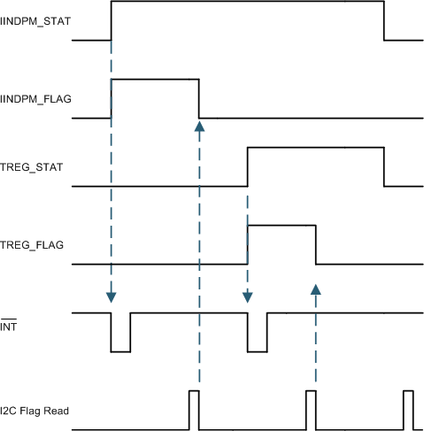
Each one of these INT sources can be masked off to prevent INT pulses from being sent out when they occur. Three bits exist for each one of these events:
- The STAT bit holds the current status of each INT source
- The FLAG bit holds information on which source produced an INT, regardless of current status.
- The MASK bit is used to prevent the device from sending out INT for each particular event.
When one of the above conditions occurs, the device sends out an INT pulse and keeps track of which source generated the INT via the FLAG registers. The FLAG register bits are automatically reset to zero after the host reads them, and a new edge on STAT bit is required to re-assert the FLAG.
 Figure 21. INT Generation Behavior Example