SLUSC16B November   2015  – March 2019

PRODUCTION DATA.  

  1. Features
  2. Applications
  3. Description
    1.     Device Images
      1.      Simplified Schematic
  4. Revision History
  5. Pin Configuration and Functions
    1.     Pin Functions
  6. Specifications
    1. 6.1 Absolute Maximum Ratings
    2. 6.2 ESD Ratings
    3. 6.3 Recommended Operating Conditions
    4. 6.4 Thermal Information
    5. 6.5 Electrical Characteristics
    6. 6.6 Timing Requirements
    7. 6.7 Typical Characteristics
  7. Detailed Description
    1. 7.1 Overview
    2. 7.2 Functional Block Diagram
    3. 7.3 Feature Description
      1. 7.3.1 Charge Pump Control
      2. 7.3.2 Pin Enable Controls
        1. 7.3.2.1 External Control of CHG and DSG Output Drivers
        2. 7.3.2.2 External Control of PCHG Output Driver
        3. 7.3.2.3 Pack Monitor Enable
    4. 7.4 Device Functional Modes
  8. Application and Implementation
    1. 8.1 Application Information
      1. 8.1.1 Recommended System Implementation
        1. 8.1.1.1 bq76200 Slave Device
        2. 8.1.1.2 Flexible Control via AFE or via MCU
        3. 8.1.1.3 Scalable VDDCP Capacitor to Support Multiple FETs in Parallel
        4. 8.1.1.4 Precharge and Predischarge Support
        5. 8.1.1.5 Optional External Gate Resistor
        6. 8.1.1.6 Separate Charge and Discharge paths
    2. 8.2 Typical Applications
      1. 8.2.1 Design Requirements
      2. 8.2.2 Detailed Design Procedure
      3. 8.2.3 Application Curves
  9. Power Supply Recommendations
  10. 10Layout
    1. 10.1 Layout Guidelines
    2. 10.2 Layout Example
  11. 11Device and Documentation Support
    1. 11.1 Documentation Support
      1. 11.1.1 Related Documentation
    2. 11.2 Community Resources
    3. 11.3 Trademarks
    4. 11.4 Electrostatic Discharge Caution
    5. 11.5 Glossary
  12. 12Mechanical, Packaging, and Orderable Information

Package Options

Mechanical Data (Package|Pins)
Thermal pad, mechanical data (Package|Pins)
Orderable Information

Application Curves

bq76200 scope1.png
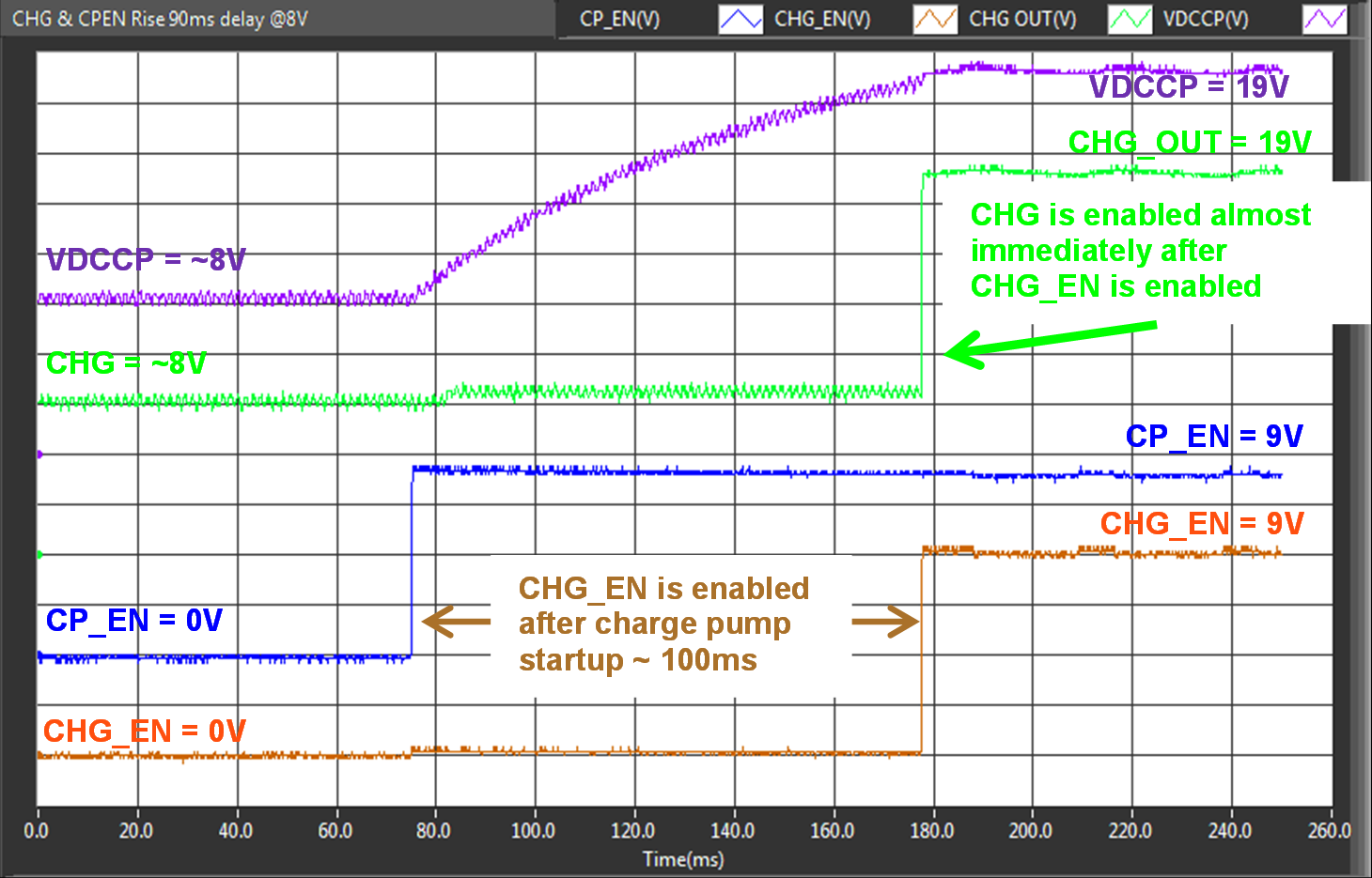
CHG output reacts to the CHG_EN signal immediately. Similar behavior applies to the DSG pin.
Figure 12. CHG_EN Switched On After Charger Pump Turns On and Is Stable
bq76200 scope3.png
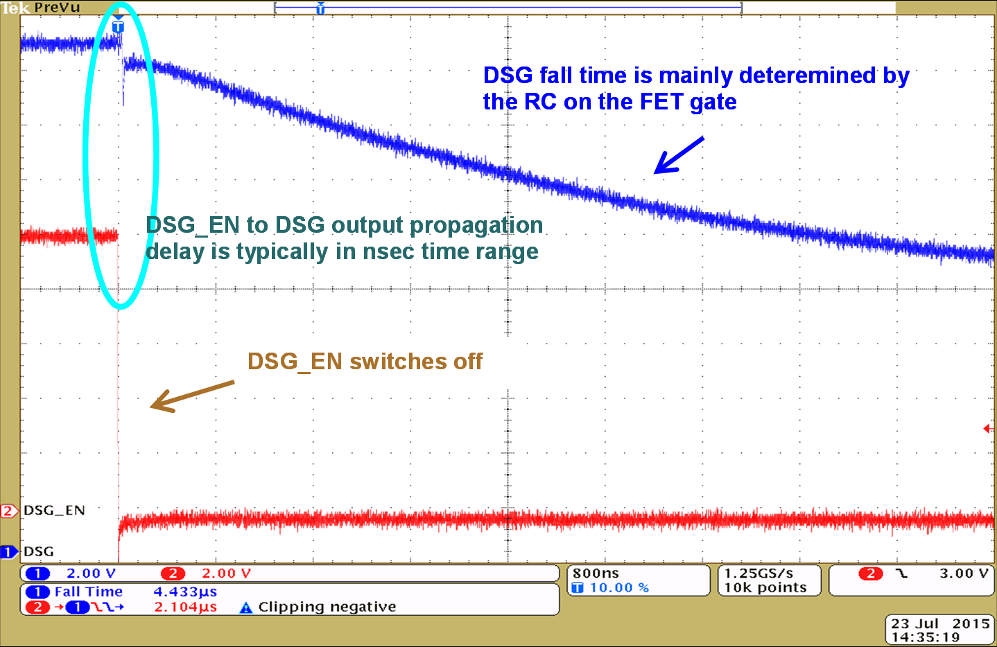
With 10-nF loading and no Rgs on DSG output. Note the time scale was 800 ns/div; thus, the DSG waveform above is basically the DSG FET fall time.
Figure 14. DSG_EN to DSG Output Propagation Delay
bq76200 scope2.png
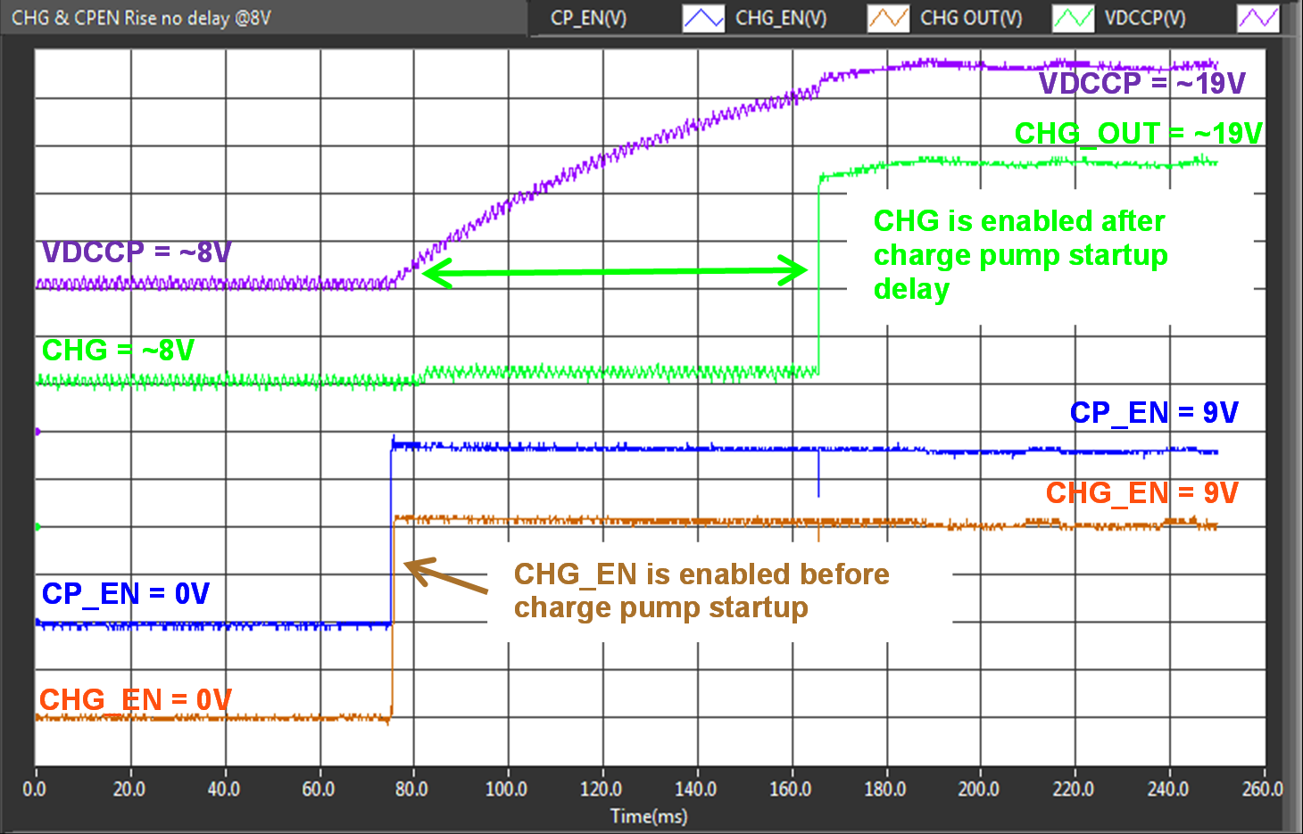
CHG output reacts to the CHG_EN signal after charge pump startup delay. Similar behavior applies to the DSG pin.
Figure 13. CHG_EN Enabled Before Charge Pump is Turned On