SLPS422B March 2013 – August 2016 CSD97376Q4M
PRODUCTION DATA.
- 1 Features
- 2 Applications
- 3 Description
- 4 Revision History
- 5 Pin Configuration and Functions
- 6 Specifications
- 7 Detailed Description
- 8 Application and Implementation
- 9 Layout
- 10Device and Documentation Support
- 11Mechanical, Packaging, and Orderable Information
Package Options
Mechanical Data (Package|Pins)
- DPC|8
Thermal pad, mechanical data (Package|Pins)
Orderable Information
8.5.3 Calculating SOA Adjustments
- SOA adjustment for switching frequency ≈ -0.2°C (Figure 6)
- SOA adjustment for input voltage ≈ 2.5°C (Figure 7)
- SOA adjustment for output voltage ≈ 1°C (Figure 8)
- SOA adjustment for output inductor ≈ 2.3°C (Figure 9)
- Final calculated SOA adjustment = -0.2 + 2.5 + (-1.5) + 2.3 ≈ 3.1°C

| VIN = 12 V | VDD = 5 V | VOUT = 1.8 V | ƒSW = 500 kHz | LOUT = 0.29 µH |
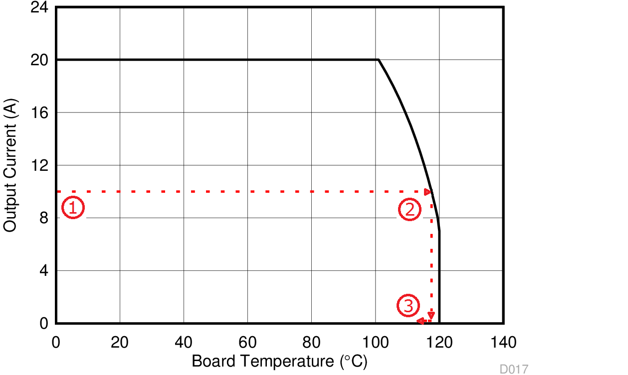
In the design example above, the estimated power loss of the CSD97376Q4M would increase to 2.3 W. In addition, the maximum allowable board and/or ambient temperature would have to decrease by 3.1°C. Figure 16 graphically shows how the SOA curve would be adjusted accordingly.
- Start by drawing a horizontal line from the application current to the SOA curve.
- Draw a vertical line from the SOA curve intercept down to the board/ambient temperature.
- Adjust the SOA board/ambient temperature by subtracting the temperature adjustment value.
In the design example, the SOA temperature adjustment yields a reduction in allowable board/ambient temperature of 3.1°C. In the event the adjustment value is a negative number, subtracting the negative number would yield an increase in allowable board/ambient temperature.