SLPS422B March   2013  – August 2016 CSD97376Q4M

PRODUCTION DATA.  

  1. Features
  2. Applications
  3. Description
    1.     Device Images
      1.      Application Diagram
      2.      Typical Power Stage Efficiency and Power Loss
  4. Revision History
  5. Pin Configuration and Functions
    1.     Pin Functions
  6. Specifications
    1. 6.1 Absolute Maximum Ratings
    2. 6.2 ESD Ratings
    3. 6.3 Recommended Operating Conditions
    4. 6.4 Thermal Information
    5. 6.5 Electrical Characteristics
    6. 6.6 Typical Characteristics
  7. Detailed Description
    1. 7.1 Functional Block Diagram
    2. 7.2 Powering CSD97376Q4M and Gate Drivers
    3. 7.3 Undervoltage Lockout Protection (UVLO)
    4. 7.4 PWM Pin
    5. 7.5 SKIP# Pin
      1. 7.5.1 Zero Crossing (ZX) Operation
    6. 7.6 Integrated Boost-Switch
  8. Application and Implementation
    1. 8.1 Application Information
    2. 8.2 Power Loss Curves
    3. 8.3 Safe Operating Curves (SOA)
    4. 8.4 Normalized Curves
    5. 8.5 Calculating Power Loss and SOA
      1. 8.5.1 Design Example
      2. 8.5.2 Calculating Power Loss
      3. 8.5.3 Calculating SOA Adjustments
  9. Layout
    1. 9.1 Layout Guidelines
      1. 9.1.1 Recommended PCB Design Overview
      2. 9.1.2 Electrical Performance
      3. 9.1.3 Thermal Performance
    2. 9.2 Layout Example
  10. 10Device and Documentation Support
    1. 10.1 Receiving Notification of Documentation Updates
    2. 10.2 Community Resources
    3. 10.3 Trademarks
    4. 10.4 Electrostatic Discharge Caution
    5. 10.5 Glossary
  11. 11Mechanical, Packaging, and Orderable Information
    1. 11.1 Package Dimensions
    2. 11.2 Recommended PCB Land Pattern
    3. 11.3 Recommended Stencil Opening

Package Options

Mechanical Data (Package|Pins)
  • DPC|8
Thermal pad, mechanical data (Package|Pins)
Orderable Information

Undervoltage Lockout Protection (UVLO)

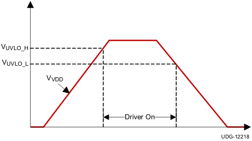
The undervoltage lockout (UVLO) comparator evaluates the VDD voltage level. As VVDD rises, both the control FET and sync FET gates hold actively low at all times until VVDD reaches the higher UVLO threshold (VUVLO_H). Then the driver becomes operational and responds to PWM and SKIP# commands. If VDD falls below the lower UVLO threshold (VUVLO_L = VUVLO_H – hysteresis), the device disables the driver and drives the outputs of the control FET and sync FET gates actively low. Figure 13 shows this function.

CAUTION

Do not start the driver in the very low power mode (SKIP# = tri-state).
CSD97376Q4M v12218_lusba6.gifFigure 13. UVLO Operation