SLAS528B August 2017 – January 2018 DAC5672A
PRODUCTION DATA.
- 1 Features
- 2 Applications
- 3 Description
- 4 Revision History
- 5 Pin Configuration and Functions
-
6 Specifications
- 6.1 Absolute Maximum Ratings
- 6.2 ESD Ratings
- 6.3 Recommended Operating Conditions
- 6.4 Thermal Information
- 6.5 Electrical Characteristics
- 6.6 Electrical Characteristics
- 6.7 Electrical Characteristics: AC Characteristics
- 6.8 Electrical Characteristics: Digital Characteristics
- 6.9 Switching Characteristics
- 6.10 Typical Characteristics
- 7 Detailed Description
- 8 Application and Implementation
- 9 Power Supply Recommendations
- 10Layout
- 11Device and Documentation Support
- 12Mechanical, Packaging, and Orderable Information
Package Options
Mechanical Data (Package|Pins)
- PFB|48
Thermal pad, mechanical data (Package|Pins)
Orderable Information
8 Application and Implementation
NOTE
Information in the following applications sections is not part of the TI component specification, and TI does not warrant its accuracy or completeness. TI’s customers are responsible for determining suitability of components for their purposes. Customers should validate and test their design implementation to confirm system functionality.
8.2 Typical Application
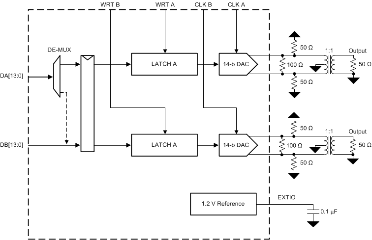
A typical application for the DAC5672A is as dual or single carrier transmitter. The DAC is provided with some input digital baseband signal and it outputs an analog carrier. A typical configuration is described below.
 Figure 25. Typical Application Schematic
- Clock rate = 122.88 MHz
- Input data = WCDMA with IF frequency at 30.72 MHz
- AVDD= DVDD = 3.3 V
8.2.1 Design Requirements
The requirements for this design were to generate a single WCDMA signal at an intermediate frequency of 30.72 MHz. The ACLR needs to be better than 72 dBc.
8.2.2 Detailed Design Procedure
The single carrier signal with an intermediate frequency of 30.72 MHz must be created in the digital processor at a sample rate of 122.88 Msps for DAC. These 14 bit samples are placed on the 14b CMOS input port of the DAC.
A CMOS DAC clock must be generated from a clock source at 122.88 MHz. This must be provided to the CLK pin of the DAC.
The IOUTA and IOUTB differential connections must be connected to a transformer to provide a single ended output. A typical 1:1 impedance transformer is used on the device EVM. The DAC5672A EVM provides a good reference for this design example.
8.2.3 Application Curves
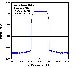
This spectrum analyzer plot shows the ACLR for the transformer output single carrier signal with intermediate frequency of 30.72 MHz. The results meet the system requirements for a minimum of 72 dBc ACLR.
 Figure 26. TBD