SLAS528B August 2017 – January 2018 DAC5672A
PRODUCTION DATA.
- 1 Features
- 2 Applications
- 3 Description
- 4 Revision History
- 5 Pin Configuration and Functions
-
6 Specifications
- 6.1 Absolute Maximum Ratings
- 6.2 ESD Ratings
- 6.3 Recommended Operating Conditions
- 6.4 Thermal Information
- 6.5 Electrical Characteristics
- 6.6 Electrical Characteristics
- 6.7 Electrical Characteristics: AC Characteristics
- 6.8 Electrical Characteristics: Digital Characteristics
- 6.9 Switching Characteristics
- 6.10 Typical Characteristics
- 7 Detailed Description
- 8 Application and Implementation
- 9 Power Supply Recommendations
- 10Layout
- 11Device and Documentation Support
- 12Mechanical, Packaging, and Orderable Information
Package Options
Mechanical Data (Package|Pins)
- PFB|48
Thermal pad, mechanical data (Package|Pins)
Orderable Information
7 Detailed Description
7.1 Overview
The architecture of the DAC5672A uses a current steering technique to enable fast switching and high update rate. The core element within the monolithic DAC is an array of segmented current sources that are designed to deliver a full-scale output current of up to 20 mA. An internal decoder addresses the differential current switches each time the DAC is updated and a corresponding output current is formed by steering all currents to either output summing node, IOUT1 or IOUT2. The complementary outputs deliver a differential output signal, which improves the dynamic performance through reduction of even-order harmonics, common-mode signals (noise), and double the peak-to-peak output signal swing by a factor of two, as compared to single-ended operation.
The segmented architecture results in a significant reduction of the glitch energy and improves the dynamic performance (SFDR) and DNL. The current outputs maintain a very high output impedance of greater
than 300 kΩ.
When pin 42 (GSET) is high (simultaneous gain set mode), the full-scale output current for DACs is determined by the ratio of the internal reference voltage (1.2 V) and an external resistor (RSET) connected to BIASJ_A. When GSET is low (independent gain set mode), the full-scale output current for each DAC is determined by the ratio of the internal reference voltage (1.2 V) and separate external resistors (RSET) connected to BIASJ_A and BIASJ_B. The resulting IREF is internally multiplied by a factor of 32 to produce an effective DAC output current that can range from 2 mA to 20 mA, depending on the value of RSET.
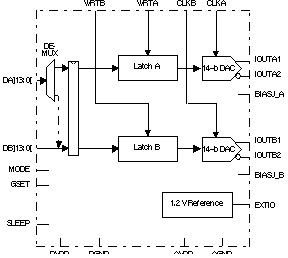
The DAC5672A is split into a digital and an analog portion, each of which is powered through its own supply pin. The digital section includes edge-triggered input latches and the decoder logic, while the analog section comprises both the current source array with its associated switches, and the reference circuitry.
7.2 Functional Block Diagram
7.3 Feature Description
7.3.1 Input Interfaces
The DAC5672A features two operating modes selected by the MODE pin, as shown in Table 1.
- For dual-bus input mode, the device essentially consists of two separate DACs. Each DAC has its own separate data input bus, clock input, and data write signal (data latch-in).
- In single-bus interleaved mode, the data must be presented interleaved at the A-channel input bus. The B-channel input bus is not used in this mode. The clock and write input are now shared by both DACs.
7.3.2 Dual-Bus Data Interface and Timing
In dual-bus mode, the MODE pin is connected to DVDD. The two converter channels within the DAC5672A consist of two independent, 14-bit, parallel data ports. Each DAC channel is controlled by its own set of write (WRTA, WRTB) and clock (CLKA, CLKB) lines. The WRTA, WRTB lines control the channel input latches and the CLKA, CLKB lines control the DAC latches. The data is first loaded into the input latch by a rising edge of the WRTA, WRTB line.
The internal data transfer requires a correct sequence of write and clock inputs, since essentially two clock domains having equal periods (but possibly different phases) are input to the DAC5672A. The DAC5672A is defined by a minimum requirement of the time between the rising edge of the clock and the rising edge of the write inputs. The rising edge of CLKA, CLKB must occur at the same time or before the rising edge of the WRTA, WRTB signal. A minimum delay of 2 ns must be maintained if the rising edge of the clock occurs after the rising edge of the write. Note that these conditions are satisfied when the clock and write inputs are connected externally. Note that all specifications were measured with the WRTA, WRTB and CLKA, CLKB lines connected together.
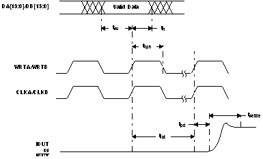 Figure 17. Dual-Bus Mode Operation
7.3.3 Single-Bus Interleaved Data Interface and Timing
In single-bus interleaved mode, the MODE pin is connected to DGND. Figure 18 shows the timing diagram. In interleaved mode, the A- and B-channels share the write input (WRTIQ) and update clock (CLKIQ and internal CLKDACIQ). Multiplexing logic directs the input word at the A-channel input bus to either the A-channel input latch (SELECTIQ is high) or to the B-channel input latch (SELECTIQ is low). When SELECTIQ is high, the data value in the B-channel latch is retained by presenting the latch output data to its input again. When SELECTIQ is low, the data value in the A-channel latch is retained by presenting the latch output data to its input.
In interleaved mode, the A-channel input data rate is twice the update rate of the DAC core. As in dual-bus mode, it is important to maintain a correct sequence of write and clock inputs. The edge-triggered flip-flops latch the A- and B-channel input words on the rising edge of the write input (WRTIQ). This data is presented to the A- and B-DAC latches on the following falling edge of the write inputs. The DAC5672A clock input is divided by a factor of two before it is presented to the DAC latches.
Correct pairing of the A- and B-channel data is done by RESETIQ. In interleaved mode, the clock input CLKIQ is divided by two, which would translate to a non-deterministic relation between the rising edges of the CLKIQ and CLKDACIQ. RESETIQ ensures, however, that the correct position of the rising edge of CLKDACIQ with respect to the data at the input of the DAC latch is determined. CLKDACIQ is disabled (low) when RESETIQ is high.
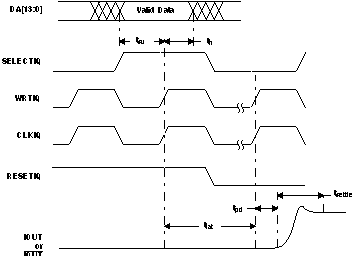 Figure 18. Single-Bus Interleaved Mode Operation
7.4 Device Functional Modes
7.4.1 DAC Transfer Function
Each of the DACs in the DAC5672A has a set of complementary current outputs, IOUT1 and IOUT2. The full-scale output current, IOUTFS, is the summation of the two complementary output currents:

The individual output currents depend on the DAC code and can be expressed as:


where Code is the decimal representation of the DAC data input word. Additionally, IOUTFS is a function of the reference current IREF, which is determined by the reference voltage and the external setting resistor (RSET).

In most cases, the complementary outputs drive resistive loads or a terminated transformer. A signal voltage develops at each output according to:


The value of the load resistance is limited by the output compliance specification of the DAC5672A. To maintain specified linearity performance, the voltage for IOUT1 and IOUT2 must not exceed the maximum allowable compliance range.
The total differential output voltage is:


7.4.2 Analog Outputs
The DAC5672A provides two complementary current outputs, IOUT1 and IOUT2. The simplified circuit of the analog output stage representing the differential topology is shown in Figure 19. The output impedance of IOUT1 and IOUT2 results from the parallel combination of the differential switches, along with the current sources and associated parasitic capacitances.
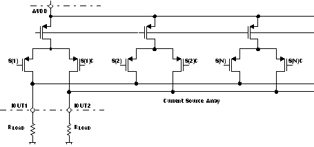 Figure 19. Analog Outputs
The signal voltage swing that may develop at the two outputs, IOUT1 and IOUT2, is limited by a negative and positive compliance. The negative limit of –1 V is given by the breakdown voltage of the CMOS process and exceeding it compromises the reliability of the DAC5672A (or even causes permanent damage). With the full-scale output set to 20 mA, the positive compliance equals 1.2 V. Note that the compliance range decreases to about 1 V for a selected output current of IOUTFS = 2 mA. Care must be taken that the configuration of DAC5672A does not exceed the compliance range to avoid degradation of the distortion performance and integral linearity.
Best distortion performance is typically achieved with the maximum full-scale output signal limited to approximately 0.5 VPP. This is the case for a 50-Ω doubly-terminated load and a 20-mA full-scale output current. A variety of loads can be adapted to the output of the DAC5672A by selecting a suitable transformer while maintaining optimum voltage levels at IOUT1 and IOUT2. Furthermore, using the differential output configuration in combination with a transformer is instrumental for achieving excellent distortion performance. Common-mode errors, such as even-order harmonics or noise, can be substantially reduced. This is particularly the case with high output frequencies.
For those applications requiring the optimum distortion and noise performance, it is recommended to select a full-scale output of 20 mA. A lower full-scale range of 2 mA may be considered for applications that require low power consumption, but can tolerate a slight reduction in performance level.
7.4.3 Output Configurations
The current outputs of the DAC5672A allow for a variety of configurations. As mentioned previously, utilizing the converter’s differential outputs yield the best dynamic performance. Such a differential output circuit may consist of an RF transformer or a differential amplifier configuration. The transformer configuration is ideal for most applications with ac coupling, while op amps are suitable for a dc-coupled configuration.
The single-ended configuration may be considered for applications requiring a unipolar output voltage. Connecting a resistor from either one of the outputs to ground converts the output current into a ground-referenced voltage signal. To improve on the dc linearity by maintaining a virtual ground, an I-to-V or op-amp configuration may be considered.
7.4.4 Differential With Transformer
Using an RF transformer provides a convenient way of converting the differential output signal into a single-ended signal while achieving excellent dynamic performance. The appropriate transformer must be carefully selected based on the output frequency spectrum and impedance requirements.
The differential transformer configuration has the benefit of significantly reducing common-mode signals, thus improving the dynamic performance over a wide range of frequencies. Furthermore, by selecting a suitable impedance ratio (winding ratio) the transformer can provide optimum impedance matching while controlling the compliance voltage for the converter outputs.
Figure 20 and Figure 21 show 50-Ω doubly-terminated transformer configurations with 1:1 and 4:1 impedance ratios, respectively. Note that the center tap of the primary input of the transformer has to be grounded to enable a dc-current flow. Applying a 20-mA full-scale output current would lead to a 0.5-VPP output for a 1:1 transformer and a 1-VPP output for a 4:1 transformer. In general, the 1:1 transformer configuration will have slightly better output distortion, but the 4:1 transformer will have 6 dB higher output power.
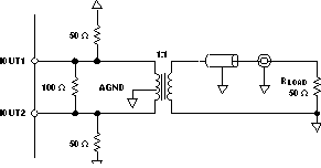 Figure 20. Driving a Doubly-Terminated 50-Ω Cable Using a 1:1 Impedance Ratio Transformer
 Figure 21. Driving a Doubly-Terminated 50-Ω Cable Using a 4:1 Impedance Ratio Transformer
7.4.5 Single-Ended Configuration
Figure 22 shows the single-ended output configuration, where the output current IOUT1 flows into an equivalent load resistance of 25 Ω. Node IOUT2 must be connected to AGND or terminated with a resistor of 25 Ω to AGND. The nominal resistor load of 25 Ω gives a differential output swing of 1 VPP when applying a 20-mA full-scale output current.
 Figure 22. Driving a Doubly-Terminated 50-Ω Cable Using a Single-Ended Output
7.4.6 Reference Operation
7.4.6.1 Internal Reference
The DAC5672A has an on-chip reference circuit which comprises a 1.2-V bandgap reference and two control amplifiers, one for each DAC. The full-scale output current, IOUTFS, of the DAC5672A is determined by the reference voltage, VREF, and the value of resistor RSET. IOUTFS can be calculated by:

The reference control amplifier operates as a V-to-I converter producing a reference current, IREF, which is determined by the ratio of VREF and RSET (see Equation 9). The full-scale output current, IOUTFS, results from multiplying IREF by a fixed factor of 32.
Using the internal reference, a 2-kΩ resistor value results in a full-scale output of approximately 20 mA. Resistors with a tolerance of 1% or better should be considered. Selecting higher values, the output current can be adjusted from 20 mA down to 2 mA. Operating the DAC5672A at lower than 20-mA output currents may be desirable for reasons of reducing the total power consumption, improving the distortion performance, or observing the output compliance voltage limitations for a given load condition.
It is recommended to bypass the EXTIO pin with a ceramic chip capacitor of 0.1 μF or more. The control amplifier is internally compensated and its small signal bandwidth is approximately 300 kHz.
7.4.6.2 External Reference
The internal reference can be disabled by simply applying an external reference voltage into the EXTIO pin, which in this case functions as an input. The use of an external reference may be considered for applications that require higher accuracy and drift performance or to add the ability of dynamic gain control.
While a 0.1-μF capacitor is recommended to be used with the internal reference, it is optional for the external reference operation. The reference input, EXTIO, has a high input impedance (1 MΩ) and can easily be driven by various sources. Note that the voltage range of the external reference must stay within the compliance range of the reference input.
7.4.6.3 Gain Setting Option
The full-scale output current on the DAC5672A can be set two ways: either for each of the two DAC channels independently or for both channels simultaneously. For the independent gain set mode, the GSET pin (pin 42) must be low (that is, connected to AGND). In this mode, two external resistors are required — one RSET connected to the BIASJ_A pin (pin 44) and the other to the BIASJ_B pin (pin 41). In this configuration, the user has the flexibility to set and adjust the full-scale output current for each DAC independently, allowing for the compensation of possible gain mismatches elsewhere within the transmit signal path.
Alternatively, bringing the GSET pin high (that is, connected to AVDD), the DAC5672A switches into the simultaneous gain set mode. Now the full-scale output current of both DAC channels is determined by only one external RSET resistor connected to the BIASJ_A pin. The resistor at the BIASJ_B pin may be removed; however, this is not required since this pin is not functional in this mode and the resistor has no effect on the gain equation.
7.4.6.4 Sleep Mode
The DAC5672A features a power-down function which can reduce the total supply current to approximately 3.1 mA over the specified supply range if no clock is present. Applying a logic high to the SLEEP pin initiates the power-down mode, while a logic low enables normal operation. When left unconnected, an internal active pulldown circuit enables the normal operation of the converter.
7.5 Programming
7.5.1 Digital Inputs and Timing
7.5.1.1 Digital Inputs
The data input ports of the DAC5672A accept a standard positive coding with data bits DA13 and DB13 being the most significant bits (MSB). The converter outputs support a clock rate of up to 275 MSPS. The best performance is typically achieved with a symmetric duty cycle for write and clock; however, the duty cycle may vary as long as the timing specifications are met. Similarly, the setup and hold times may be chosen within their specified limits.
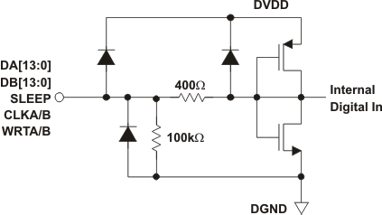
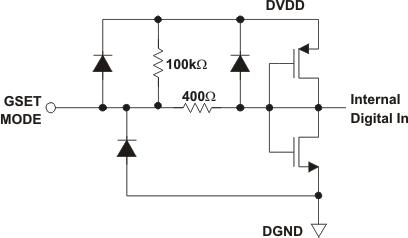
All digital inputs of the DAC5672A are CMOS compatible. Figure 23 and Figure 24 show schematics of the equivalent CMOS digital inputs of the DAC5672A. The pullup and pulldown circuitry is approximately equivalent to 100 kΩ. The 14-bit digital data input follows the offset positive binary coding scheme. The DAC5672A is designed to operate with a digital supply (DVDD) of 3 V to 3.6 V.
