SLAS528B August   2017  – January 2018 DAC5672A

PRODUCTION DATA.  

  1. Features
  2. Applications
  3. Description
  4. Revision History
  5. Pin Configuration and Functions
  6. Specifications
    1. 6.1  Absolute Maximum Ratings
    2. 6.2  ESD Ratings
    3. 6.3  Recommended Operating Conditions
    4. 6.4  Thermal Information
    5. 6.5  Electrical Characteristics
    6. 6.6  Electrical Characteristics
    7. 6.7  Electrical Characteristics: AC Characteristics
    8. 6.8  Electrical Characteristics: Digital Characteristics
    9. 6.9  Switching Characteristics
    10. 6.10 Typical Characteristics
  7. Detailed Description
    1. 7.1 Overview
    2. 7.2 Functional Block Diagram
    3. 7.3 Feature Description
      1. 7.3.1 Input Interfaces
      2. 7.3.2 Dual-Bus Data Interface and Timing
      3. 7.3.3 Single-Bus Interleaved Data Interface and Timing
    4. 7.4 Device Functional Modes
      1. 7.4.1 DAC Transfer Function
      2. 7.4.2 Analog Outputs
      3. 7.4.3 Output Configurations
      4. 7.4.4 Differential With Transformer
      5. 7.4.5 Single-Ended Configuration
      6. 7.4.6 Reference Operation
        1. 7.4.6.1 Internal Reference
        2. 7.4.6.2 External Reference
        3. 7.4.6.3 Gain Setting Option
        4. 7.4.6.4 Sleep Mode
    5. 7.5 Programming
      1. 7.5.1 Digital Inputs and Timing
        1. 7.5.1.1 Digital Inputs
  8. Application and Implementation
    1. 8.1 Application Information
    2. 8.2 Typical Application
      1. 8.2.1 Design Requirements
      2. 8.2.2 Detailed Design Procedure
      3. 8.2.3 Application Curves
  9. Power Supply Recommendations
  10. 10Layout
    1. 10.1 Layout Guidelines
    2. 10.2 Layout Example
  11. 11Device and Documentation Support
    1. 11.1 Receiving Notification of Documentation Updates
    2. 11.2 Community Resources
    3. 11.3 Trademarks
    4. 11.4 Electrostatic Discharge Caution
    5. 11.5 Glossary
  12. 12Mechanical, Packaging, and Orderable Information

Package Options

Mechanical Data (Package|Pins)
Thermal pad, mechanical data (Package|Pins)
Orderable Information

Pin Configuration and Functions

PFB Package
48-Pin TQFP
Top View
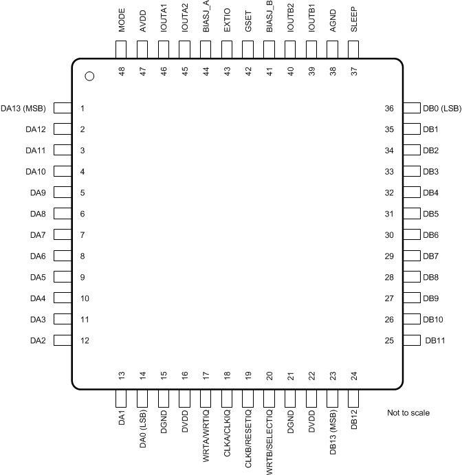
DAC5672A DAC5672_PFB_pinout.gif

Pin Functions

TERMINAL I/O DESCRIPTION
NAME NO.
AGND 38 I Analog ground
AVDD 47 I Analog supply voltage
BIASJ_A 44 O Full-scale output current bias for DACA
BIASJ_B 41 O Full-scale output current bias for DACB
CLKA/CLKIQ 18 I Clock input for DACA, CLKIQ in interleaved mode
CLKB/RESETIQ 19 I Clock input for DACB, RESETIQ in interleaved mode
DA[13:0] 1 I Data port A. DA13 is MSB and DA0 is LSB. Internal pulldown.
2
3
4
5
6
7
8
9
10
11
12
13
14
DB[13:0] 23 I Data port B. DB13 is MSB and DB0 is LSB. Internal pulldown.
24
25
26
27
28
29
30
31
32
33
34
35
36
DGND 15 I Digital ground
21
DVDD 16 I Digital supply voltage
22
EXTIO 43 I/O Internal reference output (bypass with 0.1 μF to AGND) or external reference input
GSET 42 I Gain-setting mode: H – 1 resistor, L – 2 resistors. Internal pullup.
IOUTA1 46 O DACA current output. Full-scale with all bits of DA high.
IOUTA2 45 O DACA complementary current output. Full-scale with all bits of DA low.
IOUTB1 39 O DACB current output. Full-scale with all bits of DB high.
IOUTB2 40 O DACB complementary current output. Full-scale with all bits of DB low.
MODE 48 I Mode Select: H – Dual Bus, L – Interleaved. Internal pullup.
SLEEP 37 I Sleep function control input: H – DAC in power-down mode, L – DAC in operating mode. Internal pulldown.
WRTA/WRTIQ 17 I Input write signal for PORT A (WRTIQ in interleaving mode)
WRTB/SELECTIQ 20 I Input write signal for PORT B (SELECTIQ in interleaving mode)