SLAS528B August 2017 – January 2018 DAC5672A
PRODUCTION DATA.
- 1 Features
- 2 Applications
- 3 Description
- 4 Revision History
- 5 Pin Configuration and Functions
-
6 Specifications
- 6.1 Absolute Maximum Ratings
- 6.2 ESD Ratings
- 6.3 Recommended Operating Conditions
- 6.4 Thermal Information
- 6.5 Electrical Characteristics
- 6.6 Electrical Characteristics
- 6.7 Electrical Characteristics: AC Characteristics
- 6.8 Electrical Characteristics: Digital Characteristics
- 6.9 Switching Characteristics
- 6.10 Typical Characteristics
- 7 Detailed Description
- 8 Application and Implementation
- 9 Power Supply Recommendations
- 10Layout
- 11Device and Documentation Support
- 12Mechanical, Packaging, and Orderable Information
Package Options
Mechanical Data (Package|Pins)
- PFB|48
Thermal pad, mechanical data (Package|Pins)
Orderable Information
6 Specifications
6.1 Absolute Maximum Ratings
over operating free-air temperature range (unless otherwise noted)(1)| MIN | MAX | UNIT | ||
|---|---|---|---|---|
| Supply voltage | AVDD (2) | –0.5 | 4 | V |
| DVDD (3) | ||||
| Voltage between AGND and DGND | –0.5 | 0.5 | V | |
| Voltage between AVDD and DVDD | –4 | 4 | V | |
| Supply voltage | DA [13:0] and DB [13:0] (3) | –0.5 | DVDD + 0.5 | V |
| MODE, SLEEP, CLKA, CLKB, WRTA, WRTB (3) | –0.5 | DVDD + 0.5 | V | |
| IOUTA1, IOUTA2, IOUTB1, IOUTB2 (2) | –1 | AVDD + 0.5 | V | |
| EXTIO, BIASJ_A, BIASJ_B, GSET (2) | –0.5 | AVDD + 0.5 | V | |
| Peak input current (any input) | 20 | mA | ||
| Peak total input current (all inputs) | –30 | mA | ||
| Operating free-air temperature range | –40 | 85 | °C | |
| Storage temperature, Tstg | –65 | 150 | °C | |
(1) Stresses beyond those listed under Absolute Maximum Ratings may cause permanent damage to the device. These are stress ratings only, which do not imply functional operation of the device at these or any other conditions beyond those indicated under Recommended Operating Conditions. Exposure to absolute-maximum-rated conditions for extended periods may affect device reliability.
(2) Measured with respect to AGND.
(3) Measured with respect to DGND.
6.2 ESD Ratings
| VALUE | UNIT | |||
|---|---|---|---|---|
| V(ESD) | Electrostatic discharge | Human-body model (HBM), per ANSI/ESDA/JEDEC JS-001(1) | ±2000 | V |
| Charged-device model (CDM), per JEDEC specification JESD22-C101(2) | ±1000 | |||
(1) JEDEC document JEP155 states that 500-V HBM allows safe manufacturing with a standard ESD control process.
(2) JEDEC document JEP157 states that 250-V CDM allows safe manufacturing with a standard ESD control process.
6.3 Recommended Operating Conditions
over operating free-air temperature range (unless otherwise noted)| MIN | NOM | MAX | UNIT | |||
|---|---|---|---|---|---|---|
| Supplies | ||||||
| AVDD | 3.0 | 3.3 | 3.6 | V | ||
| DVDD | 3.0 | 3.3 | 3.6 | V | ||
| I(AVDD) Analog supply current | 75 | 90 | mA | |||
| I(DVDD) Digital supply current | 25 | 38 | mA | |||
| Analog Output | ||||||
| IO(FS) Full-scale output current | 2 | 20 | mA | |||
| Output voltage compliance range | –1 | 1.25 | V | |||
| Clock Interface (CLK, CLKC) | ||||||
| CLKINPUT Frequency | 275 | MHz | ||||
6.4 Thermal Information
| THERMAL METRIC(1) | DAC5672A | UNIT | |
|---|---|---|---|
| PFB (TQFP) | |||
| 48 PINS | |||
| RθJA | Junction-to-ambient thermal resistance | 64.4 | °C/W |
| RθJC(top) | Junction-to-case (top) thermal resistance | 16.7 | °C/W |
| RθJB | Junction-to-board thermal resistance | 27.7 | °C/W |
| ψJT | Junction-to-top characterization parameter | 0.4 | °C/W |
| ψJB | Junction-to-board characterization parameter | 27.5 | °C/W |
(1) For more information about traditional and new thermal metrics, see the Semiconductor and IC Package Thermal Metrics application report.
6.5 Electrical Characteristics
over TA, AVDD = DVDD = 3.3 V, IOUTFS = 20 mA, independent gain set mode, (unless otherwise noted)| PARAMETER | TEST CONDITIONS | MIN | TYP | MAX | UNIT | |
|---|---|---|---|---|---|---|
| DC SPECIFICATIONS | ||||||
| Resolution | 14 | Bits | ||||
| DC ACCURACY (1) | ||||||
| INL | Integral nonlinearity | 1 LSB = IOUTFS / 214, TMIN to TMAX | –4 | ±1.1 | 4 | LSB |
| DNL | Differential nonlinearity | –3 | ±0.75 | 3 | LSB | |
| ANALOG OUTPUT | ||||||
| Offset error | Midscale value | ±0.03 | %FSR | |||
| Offset mismatch | Midscale value | ±0.03 | %FSR | |||
| Gain error | With external reference | ±0.25 | %FSR | |||
| With internal reference | ±0.25 | %FSR | ||||
| Minimum full-scale output current (2) | 2 | mA | ||||
| Maximum full-scale output current (2) | 20 | mA | ||||
| Gain mismatch | With external reference | –2 | 0.2 | 2 | %FSR | |
| With internal reference | –2 | 0.2 | 2 | %FSR | ||
| Output voltage compliance range (3) | –1 | 1.25 | V | |||
| RO | Output resistance | 300 | kΩ | |||
| CO | Output capacitance | 5 | pF | |||
| REFERENCE OUTPUT | ||||||
| Reference voltage | 1.14 | 1.2 | 1.26 | V | ||
| Reference output current (4) | 100 | nA | ||||
| REFERENCE INPUT | ||||||
| VEXTIO | Input voltage | 0.1 | 1.25 | V | ||
| RI | Input resistance | 1 | MΩ | |||
| Small signal bandwidth | 300 | kHz | ||||
| CI | Input capacitance | 100 | pF | |||
| TEMPERATURE COEFFICIENTS | ||||||
| Offset drift | 2 | 10 | ppm of FSR/°C | |||
| Gain drift | With external reference (DACA) | 10 | 43 | ppm of FSR/°C | ||
| With external reference (DACB) | 20 | 80 | ||||
| With internal reference | 40 | 160 | ppm of FSR/°C | |||
| Reference voltage drift | 20 | ppm /°C | ||||
(1) Measured differently through 50 Ω to AGND.
(2) Nominal full-scale current (IOUTFS) equals 32 times the IBIAS current
(3) The lower limit of the output compliance is determined by the CMOS process. Exceeding this limit may result in transistor breakdown, resulting in reduced reliability of the DAC5672A device. The upper limit of the output compliance is determined by the load resistors and ful-scale output current. Exceeding the upper limit adversely affects distortion performance and integral nonlinearity.
(4) Use an external buffer amplifier with high-impedance input to drive any external load.
6.6 Electrical Characteristics
over TA, AVDD = DVDD = 3.3 V, IOUTFS = 20 mA, fDATA = 200 MSPS, fOUT = 1 MHz, independent gain set mode, (unless otherwise noted)| PARAMETER | TEST CONDITIONS | MIN | TYP | MAX | UNIT | |
|---|---|---|---|---|---|---|
| POWER SUPPLY | ||||||
| AVDD | Analog supply voltage | 3 | 3.3 | 3.6 | V | |
| DVDD | Digital supply voltage | 3 | 3.3 | 3.6 | V | |
| IAVDD | Analog supply current | Including output current through load resistor | 75 | 90 | mA | |
| Sleep mode with clock | 2.5 | 6 | mA | |||
| Sleep mode without clock | 2.5 | mA | ||||
| IDVDD | Digital supply current | fDATA = 200 MSPS, fOUT = 1 MHz | 25 | 38 | mA | |
| Sleep mode with clock | 13.4 | 18 | mA | |||
| Sleep mode without clock | 0.6 | mA | ||||
| Power dissipation | fDATA = 200 MSPS, fOUT = 1 MHz | 330 | 390 | mW | ||
| Sleep mode with clock | 53 | |||||
| Sleep mode without clock | 9.2 | |||||
| fDATA = 275 MSPS, fOUT = 20 MHz | 350 | |||||
| APSRR | Analog power supply rejection ratio | –0.2 | –0.01 | 0.2 | %FSR/V | |
| DPSRR | Digital power supply rejection ratio | –0.2 | 0 | 0.2 | %FSR/V | |
| TA | Operating free-air temperature | –40 | 85 | °C | ||
6.7 Electrical Characteristics: AC Characteristics
AC specifications over TA , AVDD = DVDD = 3.3 V, IOUTFS = 20 mA, differential 1:1 impedance ratio transformer coupled output, 50-Ω doubly terminated load (unless otherwise noted)| PARAMETER | TEST CONDITIONS | MIN | TYP | MAX | UNIT | |
|---|---|---|---|---|---|---|
| ANALOG OUTPUT | ||||||
| fclk | Maximum output update rate (1) | 275 | MSPS | |||
| ts | Output settling time to 0.1% (DAC) | Midscale transition | 20 | ns | ||
| tr | Output rise time 10% to 90% (OUT) | 1.4 | ns | |||
| tf | Output fall time 10% to 90% (OUT) | 1.5 | ns | |||
| Output noise | IOUTFS = 20 mA | 55 | pA/√Hz | |||
| IOUTFS = 2 mA | 30 | pA/√Hz | ||||
| AC LINEARITY | ||||||
| SFDR | Spurious-free dynamic range | 1st Nyquist zone: TA = 25°C fDATA = 50 MSPS fOUT = 1 MHz IOUTFS = 0 dB |
83 | dBc | ||
| 1st Nyquist zone: TA = 25°C fDATA = 50 MSPS fOUT = 1 MHz IOUTFS = –6 dB |
80 | |||||
| 1st Nyquist zone: TA = 25°C fDATA = 50 MSPS fOUT = 1 MHz IOUTFS = –12 dB |
79 | |||||
| 1st Nyquist zone: TA = 25°C fDATA = 100 MSPS fOUT = 5 MHz |
84 | |||||
| 1st Nyquist zone, TA = 25°C, fDATA = 100 MSPS, fOUT = 20 MHz | 79 | |||||
| 1st Nyquist zone, TMIN to TMAX, fDATA = 200 MSPS, fOUT = 20 MHz | 68 | 75 | ||||
| 1st Nyquist zone, TA = 25°C, fDATA = 200 MSPS, fOUT = 41 MHz | 72 | |||||
| 1st Nyquist zone, TA = 25°C, fDATA = 275 MSPS, fOUT = 20 MHz | 74 | |||||
| SNR | Signal-to-noise ratio | 1st Nyquist zone, TA = 25°C, fDATA = 100 MSPS, fOUT = 5 MHz | 77 | dB | ||
| 1st Nyquist zone, TA = 25°C, fDATA = 160 MSPS, fOUT = 20 MHz | 70 | dB | ||||
| ACLR | Adjacent channel leakage ratio | W-CDMA signal with 3.84-MHz bandwidth, fDATA = 61.44 MSPS, IF = 15.360 MHz | 75 | dB | ||
| W-CDMA signal with 3.84-MHz bandwidth, fDATA = 122.88 MSPS, IF = 30.72 MHz | 73 | dB | ||||
| W-CDMA signal with 3.84-MHz bandwidth, fDATA = 61.44 MSPS, baseband | 78 | dB | ||||
| W-CDMA signal with 3.84-MHz bandwidth, fDATA = 122.88 MSPS, baseband | 78 | dB | ||||
| IMD3 | Third-order two-tone intermodulation | Each tone at –6 dBFS, TA = 25°C, fDATA = 200 MSPS, fOUT = 45.4 MHz and 46.4 MHz | 65 | dBc | ||
| Each tone at –6 dBFS, TA = 25°C, fDATA = 100 MSPS, fOUT = 15.1 MHz and 16.1 MHz | 79 | dBc | ||||
| IMD | Four-tone intermodulation | Each tone at –12 dBFS, TA = 25°C, fDATA = 100 MSPS, fOUT = 15.6, 15.8, 16.2, and 16.4 MHz | 79 | dBc | ||
| Each tone at –12 dBFS, TA = 25°C, fDATA = 165 MSPS, fOUT = 68.8, 69.6, 71.2, and 72 MHz | 61 | dBc | ||||
| Each tone at –12 dBFS, TA = 25°C, fDATA = 165 MSPS, fOUT = 19, 19.1, 19.3, and 19.4 MHz | 73 | dBc | ||||
| Channel isolation | TA = 25°C, fDATA = 165 MSPS, fOUT (CH1) = 20 MHz, fOUT (CH2) = 21 MHz | 95 | dBc | |||
(1)
6.8 Electrical Characteristics: Digital Characteristics
Digital specifications over TA, AVDD = DVDD = 3.3 V, IOUTFS = 20 mA, (unless otherwise noted)| PARAMETER | TEST CONDITIONS | MIN | TYP | MAX | UNIT | |
|---|---|---|---|---|---|---|
| DIGITAL INPUT | ||||||
| VIH | High-level input voltage | 2 | 3.3 | V | ||
| VIL | Low-level input voltage | 0 | 0.8 | V | ||
| IIH | High-level input current | ±50 | 0.8 | µA | ||
| IIL | Low-level input current | ±10 | µA | |||
| IIH(GSET) | High-level input current, GSET pin | 7 | µA | |||
| IIL(GSET) | Low-level input current, GSET pin | –80 | µA | |||
| IIH(MODE) | High-level input current, MODE pin | –30 | µA | |||
| IIL(MODE) | Low-level input current, MODE pin | –80 | µA | |||
| CI | Input capacitance | 5 | pF | |||
6.9 Switching Characteristics
digital specifications over TA, AVDD = DVDD = 3.3 V, IOUTFS = 20 mA, (unless otherwise noted)| PARAMETER | TEST CONDITIONS | MIN | TYP | MAX | UNIT | |
|---|---|---|---|---|---|---|
| tsu | Input setup time | Dual bus mode | 1 | ns | ||
| Single-bus interleaved mode | 0.5 | |||||
| th | Input hold time | Dual bus mode | 1 | ns | ||
| Single-bus interleaved mode | 0.5 | |||||
| tLPH | Input clock pulse high time | Dual bus mode | 1 | ns | ||
| Single-bus interleaved mode | ||||||
| tLAT | Clock latency (WRT A/B to outputs) | Dual bus mode | 4 | 4 | clk | |
| Single-bus interleaved mode | 4 | 4 | ||||
| tPD | Propagation delay time | Dual bus mode | 1.5 | ns | ||
| Single-bus interleaved mode | 1.5 | |||||
6.10 Typical Characteristics
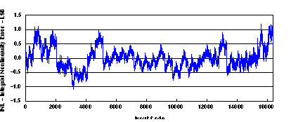 Figure 1. Integral Nonlinearity vs Input Code
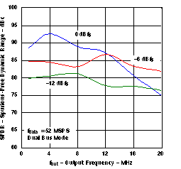 Figure 3. Spurious-Free Dynamic Range vs Output Frequency
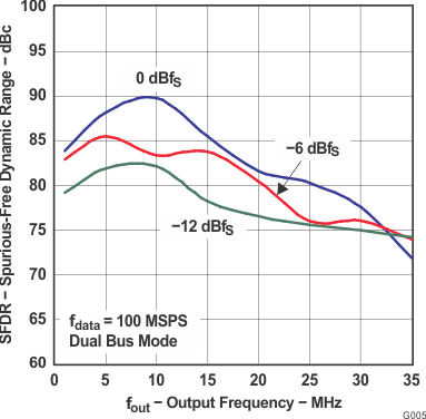 Figure 5. Spurious-Free Dynamic Range vs Output Frequency
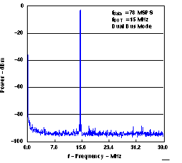 Figure 7. Single-Tone Spectrum
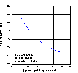 Figure 9. Two-Tone IMD3 vs Output Frequency
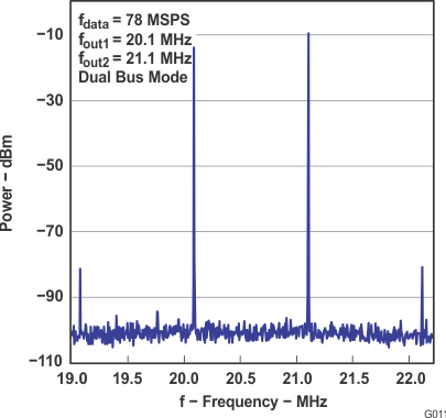 Figure 11. Two-Tone Spectrum
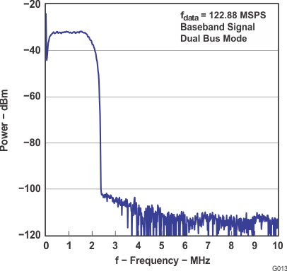 Figure 13. Power vs Frequency
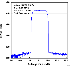 Figure 15. Power vs Frequency
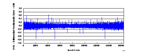 Figure 2. Differential Nonlinearity vs Input Code
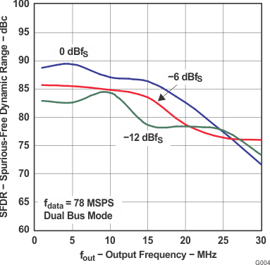 Figure 4. Spurious-Free Dynamic Range vs Output Frequency
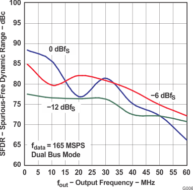 Figure 6. Spurious-Free Dynamic Range vs Output Frequency
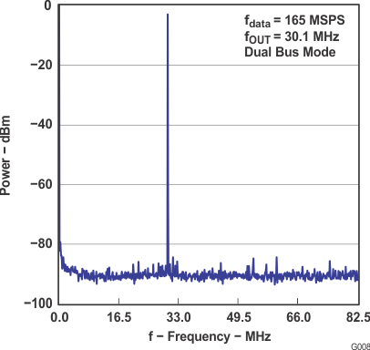 Figure 8. Single-Toned Spectrum
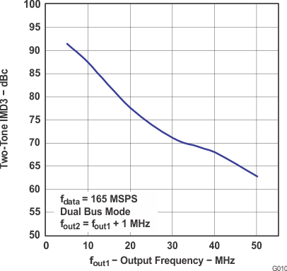 Figure 10. Two-Tone IMD3 vs Output Frequency
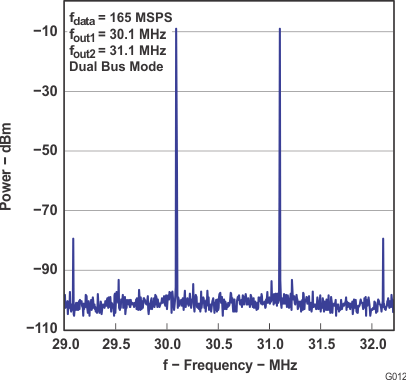 Figure 12. Two-Tone Spectrum
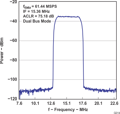 Figure 14. Power vs Frequency
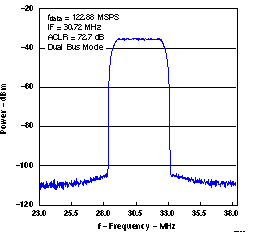 Figure 16. Power vs Frequency