SLLS853F August 2007 – January 2015 DAC5682Z
PRODUCTION DATA.
- 1 Features
- 2 Applications
- 3 Description
- 4 Revision History
- 5 Description (continued)
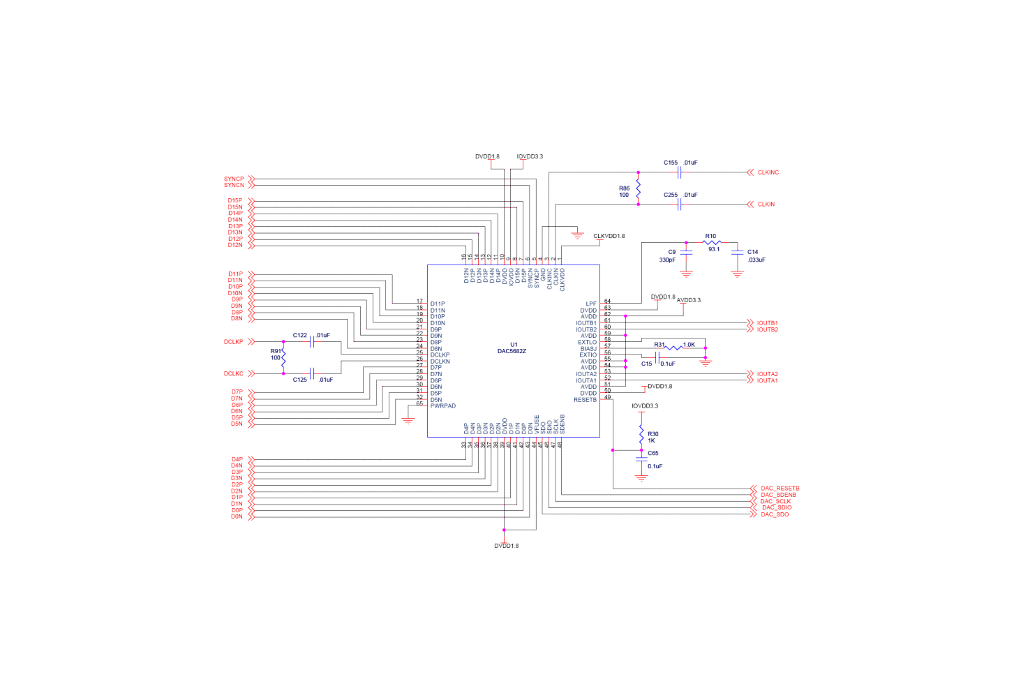
- 6 Pin Configuration and Functions
- 7 Specifications
-
8 Detailed Description
- 8.1 Overview
- 8.2 Functional Block Diagram
- 8.3
Feature Description
- 8.3.1 FIR Filters
- 8.3.2 Coarse Mixers: CMIX0 and CMIX1
- 8.3.3 Clock Inputs
- 8.3.4 LVDS Data Interfacing
- 8.3.5 LVDS Inputs
- 8.3.6 LVDS SYNCP/N Operation
- 8.3.7 DLL Operation
- 8.3.8 CMOS Digital Inputs
- 8.3.9 Reference Operation
- 8.3.10 DAC Transfer Function
- 8.3.11 DAC Output SINC Response
- 8.3.12 Analog Current Outputs
- 8.3.13 Designing the PLL Loop Filter
- 8.3.14 Test Methodology
- 8.4 Device Functional Modes
- 8.5 Programming
- 8.6
Register Maps
- 8.6.1 Register Name: STATUS0 - Address: 0x00, Default = 0x03
- 8.6.2 Register Name: CONFIG1 - Address: 0x01, Default = 0x10
- 8.6.3 Register Name: CONFIG2 - Address: 0x02, Default = 0xC0
- 8.6.4 Register Name: CONFIG3 - Address: 0x03, Default = 0x70
- 8.6.5 Register Name: STATUS4 - Address: 0x04, Default = 0x00
- 8.6.6 Register Name: CONFIG5 - Address: 0x05, Default = 0x00
- 8.6.7 Register Name: CONFIG6 - Address: 0x06, Default = 0x0C
- 8.6.8 Register Name: CONFIG7 - Address: 0x07, Default = 0xFF
- 8.6.9 Register Name: CONFIG8 - Address: 0x08, Default = 0x00
- 8.6.10 Register Name: CONFIG9 - Address: 0x09, Default = 0x00
- 8.6.11 Register Name: CONFIG10 - Address: 0x0A, Default = 0x00
- 8.6.12 Register Name: CONFIG11 - Address: 0x0B, Default = 0x00
- 8.6.13 Register Name: CONFIG12 - Address: 0x0C, Default = 0x00
- 8.6.14 Register Name: CONFIG13 - Address: 0x0D, Default = 0x00
- 8.6.15 Register Name: CONFIG14 - Address: 0x0E, Default = 0x00
- 8.6.16 Register Name: CONFIG15 - Address: 0x0F, Default = 0x00
- 9 Application and Implementation
- 10Power Supply Recommendations
- 11Layout
- 12Device and Documentation Support
- 13Mechanical, Packaging, and Orderable Information
Package Options
Refer to the PDF data sheet for device specific package drawings
Mechanical Data (Package|Pins)
- RGC|64
Thermal pad, mechanical data (Package|Pins)
- RGC|64
Orderable Information
9 Application and Implementation
NOTE
Information in the following applications sections is not part of the TI component specification, and TI does not warrant its accuracy or completeness. TI’s customers are responsible for determining suitability of components for their purposes. Customers should validate and test their design implementation to confirm system functionality.
9.1 Application Information
The DAC5682z is a high-speed, wide bandwidth Digital-to-Analog converter. The dual DAC outputs can sample at 1Gsps allowing synthesis of complex IQ signals from -400 to 400 MHz with a complex bandwidth of up to 400 MHz. When the DAC is operated in single channel bypass mode, the maximum data rate is 1Gsps and can sustain a signal bandwidth of 500 MHz. The interpolation modes of the DAC allow the input baseband rates to be 2-4 times slower than the DAC output rate reducing the processing requirements of the digital baseband processor and simplifies the DAC image filtering requirements. The coarse mixing blocks within the DAC allow power efficient placement of the final carrier at the DAC output. Typically this dual DAC with its digital features is very well equipped for complex quadrature communications applications, however it is also suitable for use in applications that require arbitrary waveform generation.
9.2 Typical Application
A typical application for the DAC5682z is a wideband transmitter. The DAC is provided with some input digital baseband signal and it outputs an analog carrier. A typical configuration is described below.
- Dual DAC mode
- Datarate = 491.52 Msps (DCLK LVPECL or LVDS)
- 2x Interpolation
- External clock mode = 983.04 MHz (CLKIN LVPECL or LVDS)
- Input data = 4C WCDMA with IF frequency at 184.32 MHz
- AVDD/IOVDD = 3.3 V
- DVDD/CLKVDD=1.8 V
- SYNCP/N = LVDS "1"
- IOUTAP/N and IOUTBP/N to transformers
9.2.1 Design Requirements
The requirements for this design were to generate a 4-carrier WCDMA signal at an intermediate frequency of 184.32 MHz. The ACPR needs to be better than 65 dBc.
9.2.2 Detailed Design Procedure
The 4-carrier signal with an intermediate frequency of 184.32 MHz must be created in the digital processor at a sample rate of 491.52 Msps for channels A and B. These 16 bit samples must be interleaved into ABAB... format and placed on the 16b LVDS input port of the DAC.
A differential DAC clock must be generated from a clock source at 983.04 MHz and a data clock at 491.52 MHz. This must be provided to the CLKIN and DCLK pins of the DAC respectively.
The DAC register map must be reset, then programmed for 2x interpolation and external clock mode as per the data sheet. The digital sample format (2s complement or offset binary) must match the incoming data from the processor. The SYNC signal must he held high for the DAC to have an analog output.
The IOUOTA and IOUTB differential connections must be connected to a transformer to provide a single ended output. A typical 2:1 impedance transformer is used on the device EVM. The DAC5682zEVM provides a good reference for this design example.
9.2.3 Application Curves
This spectrum analyzer plot shows the ACPR for the transformer output using x2 interpolation, PLL Off mode. The results meet the system requirements for a minimum of 65 dBc ACPR.
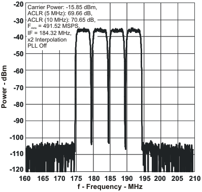 Figure 48. Four Carrier W-CDMA Test Model 1
9.3 System Examples
9.3.1 Digital Interface and Clocking Considerations for Application Examples
The DAC5682Z’s LVDS digital input bus can be driven by an FPGA or digital ASIC. This input signal can be generated directly by the FPGA, or fed by a Texas Instruments Digital Up Converter (DUC) such as the GC5016 or GC5316. Optionally, a GC1115 Crest Factor Reduction (CFR) or Digital Pre-Distortion (DPD) processor may be inserted in the digital signal chain for improving the efficiency of high-power RF amplifiers. For the details on the high-rate digital interface of the DAC, refer to LVDS Data Interfacing.
A low phase noise clock for the DAC at the final sample rate can be generated by a VCXO and a Clock Synchronizer/PLL such as the Texas Instruments CDCM7005 or CDCE62005, which can also provide other system clocks. An optional system clocking solution can use the DAC in clock multiplying PLL mode in order to avoid distributing a high-frequency clock at the DAC sample rate; however, the internal VCO phase noise of the DAC in PLL mode may degrade the quality of the DAC output signal.
9.3.2 Single Complex Input, Real IF Output Radio
Refer to Figure 49 for an example Single Complex Input, Real IF Output Radio. The DAC5682Z receives an interleaved complex I/Q baseband input data stream and increases the sample rate through interpolation by a factor of 2 or 4. By performing digital interpolation on the input data, undesired images of the original signal can be push out of the band of interest and more easily suppressed with analog filters. Complex mixing is available at each stage of interpolation using the CMIX0 and CMIX1 blocks to up-convert the signal to a frequency placement at a multiples ±Fdac/8 or ±Fdac/4. Only the real portion of the digital signal is converted by DAC-A while DAC-B can be programmed to sleep mode for reduced power consumption. The DAC output signal would typically be terminated with a transformer (see Analog Current Outputs). An IF filter, either LC or SAW, is used to suppress the DAC Nyquist zone images and other spurious signals before being mixed to RF with a mixer. The TRF3671 Frequency Synthesizer, with integrated VCO, may be used to drive the LO input of the mixer for frequencies between 375 and 2380 MHz.
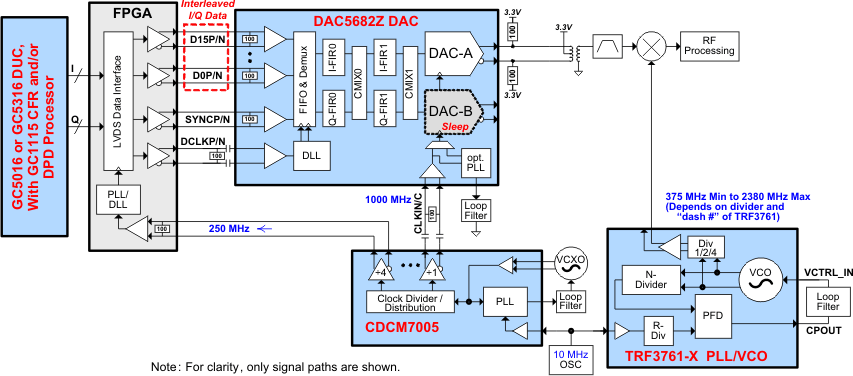 Figure 49. System Diagram of a Complex Input, Real IF Output Radio
9.3.3 Dual Channel Real IF Output Radio
Refer to Figure 50 for an example Dual-Channel Real IF Output Radio. The DAC5682Z receives an interleaved A/B input data stream and increases the sample rate through interpolation by a factor of 2 or 4. By performing digital interpolation on the input data, undesired images of the original signal can be push out of the band of interest and more easily suppressed with analog filters. Real mixing is available at each stage of interpolation using the CMIX0 and CMIX1 blocks to up-convert the signal (see Dual-Channel Real Upconversion). Both DAC output signals would typically be terminated with a transformer (see Analog Current Outputs). An IF filter, either LC or SAW, is used to suppress the DAC Nyquist zone images and other spurious signals before being mixed to RF with a mixer. The TRF3671 Frequency Synthesizer, with integrated VCO, may be used to drive a common LO input of the mixers for frequencies between 375 and 2380 MHz. Alternatively, two separate TRF3761 synthesizers could be used for independent final RF frequency placement.
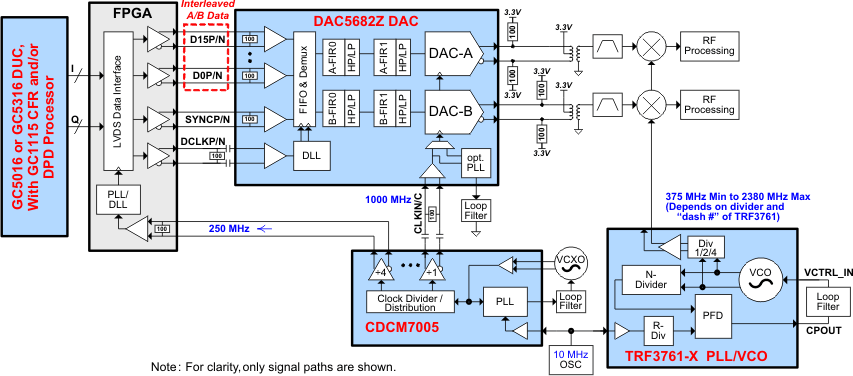 Figure 50. System Diagram of a Dual-Channel Real IF Output Radio
9.3.4 Direct Conversion Radio
Refer to Figure 51 for an example Direct Conversion Radio. The DAC5682Z receives an interleaved complex I/Q baseband input data stream and increases the sample rate through interpolation by a factor of 2 or 4. By performing digital interpolation on the input data, undesired images of the original signal can be push out of the band of interest and more easily suppressed with analog filters.
For a Zero IF (ZIF) frequency plan, complex mixing of the baseband signal is not required. Alternatively, for a Complex IF frequency plan the input data can be placed at an pre-placed at an IF within the bandwidth limitations of the interpolation filters. In addition, complex mixing is available at each stage of interpolation using the CMIX0 and CMIX1 blocks to up-convert the signal to a frequency placement at a multiples ±Fdac/8 or ±Fdac/4. The output of both DAC channels is used to produce a Hilbert transform pair and can be expressed as:
where m(t) and mh(t) connote a Hilbert transform pair and ωc is the sum of the CMIX0 and CMIX1 frequencies. The complex output is input to an analog quadrature modulator (AQM) such as the Texas Instruments TRF3703-33 for a single side-band (SSB) up conversion to RF. A passive (resistor only) interface to the AQM is recommended, with an optional LC filter network. The TRF3671 Frequency Synthesizer with integrated VCO may be used to drive the LO input of the TRF3703-33 for frequencies between 375 and 2380 MHz. Upper single-sideband upconversion is achieved at the output of the analog quadrature modulator, whose output is expressed as:
Flexibility is provided to the user by allowing for the selection of negative CMIX mixing sequences to produce a lower-sideband upconversion. Note that the process of complex mixing translates the signal frequency from 0 Hz means that the analog quadrature modulator IQ imbalance produces a sideband that falls outside the signal of interest. DC offset error in DAC and AQM signal path may produce LO feed-through at the RF output which may fall in the band of interest. To suppress the LO feed-through, the DAC5682Z provides a digital offset correction capability for both DAC-A and DAC-B paths. (See DAC_offset_ena bit in CONFIG3.)
The complex IF architecture has several advantages over the real IF architecture:
- Uncalibrated side-band suppression ~ 35 dBc compared to 0 dBc for real IF architecture.
- Direct DAC to AQM interface – no amplifiers required
- Nonharmonic clock-related spurious signals fall out-of-band
- DAC 2nd Nyquist zone image is offset fDAC compared with fDAC– 2 × IF for a real IF architecture, reducing the need for filtering at the DAC output.
- Uncalibrated LO feed through for AQM is ~ 35 dBc and calibration can reduce or completely remove the LO feed through.
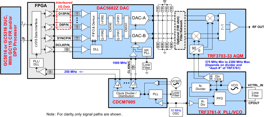 Figure 51. System Diagram of Direct Conversion Radio
9.3.5 CMTS/VOD Transmitter
The exceptional SNR of the DAC5682Z enables a dual-cable modem termination system (CMTS) or video on demand (VOD) QAM transmitter in excess of the stringent DOCSIS specification, with >74 dBc and 75 dBc in the adjacent and alternate channels.
Refer to Figure 50 for an example Dual Channel Real IF Output Radio – this signal chain is nearly identical to a typical system using the DAC5682Z for a cost optimized dual channel two QAM transmitter. A GC5016 would take four separate symbol rate inputs and provide pulse shaping and interpolation to ~ 128 MSPS. The four QAM carriers would be combined into two groups of two QAM carriers with intermediate frequencies of approximately 30 MHz to 40 MHz. The GC5016 would output two real data streams to one DAC5682Z through an FPGA for CMOS to LVDS translation. The DAC5682Z would function as a dual-channel device and provide 2x or 4x interpolation to increase the frequency of the 2nd Nyquist zone image. The two signals are then output through the two DAC outputs, through a transformer and to an RF upconverter.
9.3.6 High-Speed Arbitrary Waveform Generator
The 1GSPS bandwidth input data bus combined with the 16-bit DAC resolution of the DAC5682Z allows wideband signal generation for test and measurement applications. In this case, interpolation is not desired by the FPGA-based waveform generator as it can make use of the full Nyquist bandwidth of up to 500MHz.
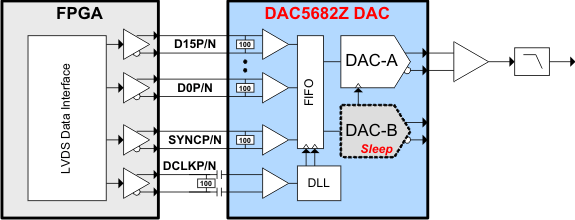 Figure 52. System Diagram of Arbitrary Waveform Generator
9.4 Initialization Set Up
9.4.1 Recommended Start-up Sequence
The following start-up sequence is recommended to initialize the DAC5682Z:
- Supply all 1.8 V (CLKVDD, DVDD, VFUSE) voltages simultaneously followed by all 3.3 V (AVDD and IOVDD) voltages.
- Provide stable CLKIN/C clock.
- Toggle RESETB pin for a minimum 25 nSec active low pulse width.
- Program all desired SIF registers. Set DLL_Restart bit during this write cycle. The CONFIG10 register value should match the corresponding DCLKP/N frequency range in the Electrical Characteristics table.
- Provide stable DCLKP/N clock. (This can also be provided earlier in the sequence)
- Clear the DLL_Restart bit when the DCLKP/N clock is expected to be stable.
- Verify the status of DLL_Lock and repeat until set to ‘1’. DLL_Lock can be monitored by reading the STATUS0 register or by monitoring the SDO pin in 3-wire SIF mode. (See description for CONFIG14 SDO_func_sel.)
- Enable transmit of data by asserting the LVDS SYNCP/N input or setting CONFIG3 SW_sync bit. (See description for CONFIG3 SW_sync and SW_sync_sel) The SYNC source must be held at a logic ‘1’ to enable data flow through the DAC. If multiple DAC devices require synchronization, refer to the "Recommended Multi-DAC Synchronization Procedure" below.
- Provide data flow to LVDS D[15:0]P/N pins. If using the LVDS SYNCP/N input, data can be input simultaneous with the logic ‘1’ transition of SYNCP/N.