SLLS853F August 2007 – January 2015 DAC5682Z
PRODUCTION DATA.
- 1 Features
- 2 Applications
- 3 Description
- 4 Revision History
- 5 Description (continued)
- 6 Pin Configuration and Functions
- 7 Specifications
-
8 Detailed Description
- 8.1 Overview
- 8.2 Functional Block Diagram
- 8.3
Feature Description
- 8.3.1 FIR Filters
- 8.3.2 Coarse Mixers: CMIX0 and CMIX1
- 8.3.3 Clock Inputs
- 8.3.4 LVDS Data Interfacing
- 8.3.5 LVDS Inputs
- 8.3.6 LVDS SYNCP/N Operation
- 8.3.7 DLL Operation
- 8.3.8 CMOS Digital Inputs
- 8.3.9 Reference Operation
- 8.3.10 DAC Transfer Function
- 8.3.11 DAC Output SINC Response
- 8.3.12 Analog Current Outputs
- 8.3.13 Designing the PLL Loop Filter
- 8.3.14 Test Methodology
- 8.4 Device Functional Modes
- 8.5 Programming
- 8.6
Register Maps
- 8.6.1 Register Name: STATUS0 - Address: 0x00, Default = 0x03
- 8.6.2 Register Name: CONFIG1 - Address: 0x01, Default = 0x10
- 8.6.3 Register Name: CONFIG2 - Address: 0x02, Default = 0xC0
- 8.6.4 Register Name: CONFIG3 - Address: 0x03, Default = 0x70
- 8.6.5 Register Name: STATUS4 - Address: 0x04, Default = 0x00
- 8.6.6 Register Name: CONFIG5 - Address: 0x05, Default = 0x00
- 8.6.7 Register Name: CONFIG6 - Address: 0x06, Default = 0x0C
- 8.6.8 Register Name: CONFIG7 - Address: 0x07, Default = 0xFF
- 8.6.9 Register Name: CONFIG8 - Address: 0x08, Default = 0x00
- 8.6.10 Register Name: CONFIG9 - Address: 0x09, Default = 0x00
- 8.6.11 Register Name: CONFIG10 - Address: 0x0A, Default = 0x00
- 8.6.12 Register Name: CONFIG11 - Address: 0x0B, Default = 0x00
- 8.6.13 Register Name: CONFIG12 - Address: 0x0C, Default = 0x00
- 8.6.14 Register Name: CONFIG13 - Address: 0x0D, Default = 0x00
- 8.6.15 Register Name: CONFIG14 - Address: 0x0E, Default = 0x00
- 8.6.16 Register Name: CONFIG15 - Address: 0x0F, Default = 0x00
- 9 Application and Implementation
- 10Power Supply Recommendations
- 11Layout
- 12Device and Documentation Support
- 13Mechanical, Packaging, and Orderable Information
Package Options
Refer to the PDF data sheet for device specific package drawings
Mechanical Data (Package|Pins)
- RGC|64
Thermal pad, mechanical data (Package|Pins)
- RGC|64
Orderable Information
6 Pin Configuration and Functions
RGC Package
64 Pins
Top View
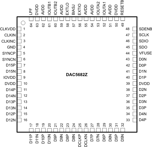
Pin Functions
| PIN | I/O | DESCRIPTION | ||
|---|---|---|---|---|
| NAME | NO. | |||
| AVDD | 51, 54, 55, 59, 62 | I | Analog supply voltage. (3.3 V) | |
| BIASJ | 57 | O | Full-scale output current bias. For 20-mA full-scale output current, connect a 960-Ω resistor to GND. | |
| CLKIN | 2 | I | Positive external clock input with a self-bias of approximately CLKVDD/2. With the clock multiplier PLL enabled, CLKIN provides lower frequency reference clock. If the PLL is disabled, CLKIN directly provides clock for DAC up to 1 GHz. | |
| CLKINC | 3 | I | Complementary external clock input. (See the CLKIN description) | |
| CLKVDD | 1 | I | Internal clock buffer supply voltage. (1.8 V) | |
| D[15..0]P | 7, 11, 13, 15, 17, 19, 21, 23, 27, 29, 31, 33, 35, 37, 40, 42 | I | LVDS positive input data bits 0 through 15. Each positive/negative LVDS pair has an internal 100 Ω termination resistor. Order of bus can be reversed via rev_bus bit in CONFIG5 register. Data format relative to DCLKP/N clock is Double Data Rate (DDR) with two data samples input per DCLKP/N clock. In dual-channel mode, data for the A-channel is input while DCLKP is high. | |
| D15P is most significant data bit (MSB) – pin 7 D0P is least significant data bit (LSB) – pin 42 |
||||
| D[15..0]N | 8, 12, 14, 16, 18, 20, 22, 24, 28, 30, 32, 34, 36, 38, 41, 43 | I | LVDS negative input data bits 0 through 15. (See D[15:0]P description above) | |
| D15N is most significant data bit (MSB) – pin 8 D0N is least significant data bit (LSB) – pin 43 |
||||
| DCLKP | 25 | I | LVDS positive input clock. Unlike the other LVDS inputs, the DCLKP/N pair is self-biased to approximately DVDD/2 and does not have an internal termination resistor in order to optimize operation of the DLL circuit. See DLL Operation. For proper external termination, connect a 100 Ω resistor across LVDS clock source lines followed by series 0.01 μF capacitors connected to each of DCLKP and DCLKN pins (see ). For best performance, the resistor and capacitors should be placed as close as possible to these pins. | |
| DCLKN | 26 | I | LVDS negative input clock. (See the DCLKP description) | |
| DVDD | 10, 39, 50, 63 | I | Digital supply voltage. (1.8 V) | |
| EXTIO | 56 | I/O | Used as external reference input when internal reference is disabled (i.e., EXTLO connected to AVDD). Used as 1.2-V internal reference output when EXTLO = GND, requires a 0.1 μF decoupling capacitor to AGND when used as reference output. | |
| EXTLO | 58 | O | Connect to GND for internal reference, or AVDD for external reference. | |
| GND | 4, Thermal Pad | I | Pin 4 and the Thermal Pad located on the bottom of the QFN package is ground for AVDD, DVDD and IOVDD supplies. | |
| IOUTA1 | 52 | O | A-Channel DAC current output. An offset binary data pattern of 0x0000 at the DAC input results in a full scale current sink and the least positive voltage on the IOUTA1 pin. Similarly, a 0xFFFF data input results in a 0 mA current sink and the most positive voltage on the IOUTA1 pin. In single DAC mode, outputs appear on the IOUTA1/A2 pair only. | |
| IOUTA2 | 53 | O | A-Channel DAC complementary current output. The IOUTA2 has the opposite behavior of the IOUTA1 described above. An input data value of 0x0000 results in a 0-mA sink and the most positive voltage on the IOUTA2 pin. | |
| IOUTB1 | 61 | O | B-Channel DAC current output. See the IOUTA1 description above. | |
| IOUTB2 | 60 | O | B-Channel DAC complementary current output. See the IOUTA2 description above. | |
| IOVDD | 9 | I | Digital I/O supply voltage (3.3 V) for pins RESETB, SCLK, SDENB, SDIO, SDO. | |
| LPF | 64 | I | PLL loop filter connection. If not using the clock multiplying PLL, the LPF pin may be left open. Set both PLL_bypass and PLL_sleep control bits for reduced power dissipation. | |
| RESETB | 49 | I | Resets the chip when low. Internal pullup. | |
| SCLK | 47 | I | Serial interface clock. Internal pulldown. | |
| SDENB | 48 | I | Active low serial data enable, always an input to the DAC5682Z. Internal pullup. | |
| SDIO | 46 | I/O | Bi-directional serial interface data in 3-pin mode (default). In 4-pin interface mode (CONFIG5 sif4), the SDIO pin is an input only. Internal pulldown. | |
| SDO | 45 | O | Uni-directional serial interface data in 4-pin mode (CONFIG5 sif4). The SDO pin is in high-impedance state in 3-pin interface mode (default), but can optionally be used as a status output pin via CONFIG14 SDO_func_sel(2:0). Internal pulldown. | |
| SYNCP | 5 | I | LVDS SYNC positive input data. The SYNCP/N LVDS pair has an internal 100 Ω termination resistor. By default, the SYNCP/N input must be logic ‘1’ to enable a DAC analog output. See the LVDS SYNCP/N Operation paragraph for a detailed description. | |
| SYNCN | 6 | I | LVDS SYNC negative input data. | |
| VFUSE | 44 | I | Digital supply voltage. (1.8 V) Connect to DVDD pins for normal operation. This supply pin is also used for factory fuse programming. | |