SLLS853F August 2007 – January 2015 DAC5682Z
PRODUCTION DATA.
- 1 Features
- 2 Applications
- 3 Description
- 4 Revision History
- 5 Description (continued)
- 6 Pin Configuration and Functions
- 7 Specifications
-
8 Detailed Description
- 8.1 Overview
- 8.2 Functional Block Diagram
- 8.3
Feature Description
- 8.3.1 FIR Filters
- 8.3.2 Coarse Mixers: CMIX0 and CMIX1
- 8.3.3 Clock Inputs
- 8.3.4 LVDS Data Interfacing
- 8.3.5 LVDS Inputs
- 8.3.6 LVDS SYNCP/N Operation
- 8.3.7 DLL Operation
- 8.3.8 CMOS Digital Inputs
- 8.3.9 Reference Operation
- 8.3.10 DAC Transfer Function
- 8.3.11 DAC Output SINC Response
- 8.3.12 Analog Current Outputs
- 8.3.13 Designing the PLL Loop Filter
- 8.3.14 Test Methodology
- 8.4 Device Functional Modes
- 8.5 Programming
- 8.6
Register Maps
- 8.6.1 Register Name: STATUS0 - Address: 0x00, Default = 0x03
- 8.6.2 Register Name: CONFIG1 - Address: 0x01, Default = 0x10
- 8.6.3 Register Name: CONFIG2 - Address: 0x02, Default = 0xC0
- 8.6.4 Register Name: CONFIG3 - Address: 0x03, Default = 0x70
- 8.6.5 Register Name: STATUS4 - Address: 0x04, Default = 0x00
- 8.6.6 Register Name: CONFIG5 - Address: 0x05, Default = 0x00
- 8.6.7 Register Name: CONFIG6 - Address: 0x06, Default = 0x0C
- 8.6.8 Register Name: CONFIG7 - Address: 0x07, Default = 0xFF
- 8.6.9 Register Name: CONFIG8 - Address: 0x08, Default = 0x00
- 8.6.10 Register Name: CONFIG9 - Address: 0x09, Default = 0x00
- 8.6.11 Register Name: CONFIG10 - Address: 0x0A, Default = 0x00
- 8.6.12 Register Name: CONFIG11 - Address: 0x0B, Default = 0x00
- 8.6.13 Register Name: CONFIG12 - Address: 0x0C, Default = 0x00
- 8.6.14 Register Name: CONFIG13 - Address: 0x0D, Default = 0x00
- 8.6.15 Register Name: CONFIG14 - Address: 0x0E, Default = 0x00
- 8.6.16 Register Name: CONFIG15 - Address: 0x0F, Default = 0x00
- 9 Application and Implementation
- 10Power Supply Recommendations
- 11Layout
- 12Device and Documentation Support
- 13Mechanical, Packaging, and Orderable Information
Package Options
Refer to the PDF data sheet for device specific package drawings
Mechanical Data (Package|Pins)
- RGC|64
Thermal pad, mechanical data (Package|Pins)
- RGC|64
Orderable Information
7 Specifications
7.1 Absolute Maximum Ratings
over operating free-air temperature range (unless otherwise noted) (1)| MIN | MAX | UNIT | ||
|---|---|---|---|---|
| Supply voltage | DVDD(2) | –0.5 | 2.3 | V |
| VFUSE(2) | –0.5 | 2.3 | V | |
| CLKVDD(2) | –0.5 | 2.3 | V | |
| AVDD(2) | –0.5 | 4 | V | |
| IOVDD(2) | –0.5 | 4 | V | |
| Supply voltage | AVDD to DVDD | –2 | 2.6 | V |
| CLKVDD to DVDD | –0.5 | 0.5 | V | |
| IOVDD to AVDD | –0.5 | 0.5 | V | |
| D[15..0]P ,D[15..0]N, SYNCP, SYNCN (2) | –0.5 | DVDD + 0.5 | V | |
| DCLKP, DCLKN(2) | –0.3 | 2.1 | V | |
| CLKIN, CLKINC(2) | –0.5 | CLKVDD + 0.5 | V | |
| SDO, SDIO, SCLK, SDENB, RESETB (2) | –0.5 | IOVDD + 0.5 | V | |
| IOUTA1/B1, IOUTA2/B2 (2) | –0.5 | AVDD + 0.5 | V | |
| LPF, EXTIO, EXTLO, BIASJ(2) | –0.5 | AVDD + 0.5 | V | |
| Peak input current (any input) | 20 | mA | ||
| Peak total input current (all inputs) | –30 | mA | ||
| Operating free-air temperature, TA: DAC5682Z | –40 | 85 | °C | |
| Storage temperature, Tstg | –65 | 150 | °C | |
(1) Stresses beyond those listed under Absolute Maximum Ratings may cause permanent damage to the device. These are stress ratings only, and functional operation of these or any other conditions beyond those indicated under Recommended Operating Conditions is not implied. Exposure to absolute-maximum-rated conditions for extended periods may affect device reliability.
(2) Measured with respect to GND.
7.2 ESD Ratings
| VALUE | UNIT | |||
|---|---|---|---|---|
| V(ESD) | Electrostatic discharge | Human body model (HBM), per ANSI/ESDA/JEDEC JS-001(1) | ±2000 | V |
| Charged-device model (CDM), per JEDEC specification JESD22-C101(2) | ±500 | |||
(1) JEDEC document JEP155 states that 500-V HBM allows safe manufacturing with a standard ESD control process.
(2) JEDEC document JEP157 states that 250-V CDM allows safe manufacturing with a standard ESD control process.
7.3 Recommended Operating Conditions
over operating free-air temperature range (unless otherwise noted)| MIN | NOM | MAX | UNIT | |
|---|---|---|---|---|
| SUPPLIES | ||||
| AVDD | 3 | 3.3 | 3.6 | V |
| DVDD | 1.7 | 1.8 | 1.9 | V |
| CLKVDD | 1.7 | 1.8 | 1.9 | V |
| IOVDD | 3 | 3.3 | 3.6 | V |
| ANALOG OUTPUT | ||||
| IOUTA1, IOUTA2, IOUTB1, IOUTB2 | 0 | 20 | 20 | mA |
| V IOUTA1, IOUTA2, IOUTB1, IOUTB2 Compliance voltage | AVDD-0.5 | AVDD+0.5 | V | |
| CLOCK INPUT | ||||
| CLKIN ECL/PECL Frequency | 1000 | MHz | ||
| CLKIN Amplitude Differential | 0.4 | 1 | CLKVDD | V |
| CLKIN Duty Cycle | 50% | |||
| CLKIN common mode voltage | CLKDVDD/2 | V | ||
| DCLK LVDS Frequency | 500 | MHz | ||
| DIGITAL INPUTS | ||||
| SYNC LVDS | 1 | 1.2 | 1.4 | V |
| D15..D0 LVDS | 1 | 1.2 | 1.4 | V |
| LVDS Common mode | 1.2 | V | ||
| LVDS Differential Swing | 0.4 | V | ||
| SCLK, SDIO, SDENB, SDO CMOS SPI | GND | IOVDD | V | |
7.4 Thermal Information
| THERMAL METRIC(1) | DAC5682Z | UNIT | |
|---|---|---|---|
| QFN | |||
| 64 PINS | |||
| TJ | Maximum junction temperature (2) | 125 | °C |
| RθJA | Theta junction-to-ambient (still air) | 22 | °C/W |
| Theta junction-to-ambient (150 lfm) | 16 | ||
| RθJC | Theta junction-to-case | 0.2 | °C/W |
| RθJP | Theta junction-to-pad | 3.5 | °C/W |
(1) For more information about traditional and new thermal metrics, see the IC Package Thermal Metrics application report, SPRA953.
(2) Air flow or heat sinking reduces θJA and may be required for sustained operation at 85° under maximum operating conditions.
7.5 Electrical Characteristics — DC Specification
over operating free-air temperature range , AVDD = 3.3 V, CLKVDD = 1.8 V, IOVDD = 3.3 V, DVDD = 1.8 V, IoutFS = 20 mA (unless otherwise noted)| PARAMETER | TEST CONDITIONS | MIN | TYP | MAX | UNIT | |
|---|---|---|---|---|---|---|
| Resolution | 16 | Bits | ||||
| DC ACCURACY(1) | ||||||
| INL | Integral nonlinearity | 1 LSB = IOUTFS/216 | ±4 | LSB | ||
| DNL | Differential nonlinearity | ±2 | ||||
| ANALOG OUTPUT | ||||||
| Course gain linearity | ±0.04 | LSB | ||||
| Offset error | Mid code offset | 0.01 | %FSR | |||
| Gain error | With external reference | 1 | %FSR | |||
| Gain error | With internal reference | 0.7 | %FSR | |||
| Gain mismatch | With internal reference, dual DAC | –2 | 2 | %FSR | ||
| Minimum full scale output current(2) | 2 | mA | ||||
| Maximum full scale output current(2) | 20 | |||||
| Output Compliance range(3) | IOUTFS = 20 mA | AVDD –0.5V |
AVDD + 0.5V |
V | ||
| Output resistance | 300 | kΩ | ||||
| Output capacitance | 5 | pF | ||||
| REFERENCE OUTPUT | ||||||
| Vref | Reference voltage | 1.14 | 1.2 | 1.26 | V | |
| Reference output current(4) | 100 | nA | ||||
| REFERENCE INPUT | ||||||
| VEXTIO | Input voltage range | 0.1 | 1.25 | V | ||
| Input resistance | 1 | MΩ | ||||
| Small signal bandwidth | CONFIG6: BiasLPF_A and BiasLPF_B = 0 | 95 | kHz | |||
| CONFIG6: BiasLPF_A and BiasLPF_B = 1 | 472 | |||||
| Input capacitance | 100 | pF | ||||
| TEMPERATURE COEFFICIENTS | ||||||
| Offset drift | ±1 | ppm of FSR/°C | ||||
| Gain drift | With external reference | ±15 | ppm of FSR/°C | |||
| With internal reference | ±30 | |||||
| Reference voltage drift | ±8 | ppm/°C | ||||
| POWER SUPPLY | ||||||
| Analog supply voltage, AVDD | 3.0 | 3.3 | 3.6 | V | ||
| Digital supply voltage, DVDD | 1.7 | 1.8 | 1.9 | V | ||
| Clock supply voltage, CLKVDD | 1.7 | 1.8 | 1.9 | V | ||
| I/O supply voltage, IOVDD | 3.0 | 3.3 | 3.6 | V | ||
| I(AVDD) | Analog supply current | Mode 4 (below) | 133 | mA | ||
| I(DVDD) | Digital supply current | 455 | mA | |||
| I(CLKVDD) | Clock supply current | 45 | mA | |||
| I(IOVDD) | IO supply current | 12 | mA | |||
| I(AVDD) | Sleep mode, AVDD supply current | Mode 6 (below) | 1.0 | mA | ||
| I(DVDD) | Sleep mode, DVDD supply current | 1.5 | mA | |||
| I(CLKVDD) | Sleep mode, CLKVDD supply current | 2.5 | mA | |||
| I(IOVDD) | Sleep mode, IOVDD supply current | 2.0 | mA | |||
| P | AVDD + IOVDD current, 3.3 V | Mode 1: 2X2, PLL = OFF, CLKIN = 983.04 MHz FDAC = 983.04 MHz, IF = 184.32 MHz DACA and DACB ON, 4 carrier WCDMA |
135 | mA | ||
| DVDD + CLKVDD current, 1.8 V | 450 | mA | ||||
| Power Dissipation | 1255 | mW | ||||
| AVDD + IOVDD current, 3.3 V | Mode 2: 2X2, PLL = ON (8X), CLKIN = 122.88 MHz FDAC = 983.04 MHz, IF = 184.32 MHz DACA and DACB ON, 4 carrier WCDMA |
145 | mA | |||
| DVDD + CLKVDD current, 1.8 V | 485 | mA | ||||
| Power Dissipation | 1350 | mW | ||||
| AVDD + IOVDD current, 3.3 V | Mode 3: 2X4, CMIX0 = Fs/4, PLL = OFF, CLKIN = 983.04 MHz FDAC = 983.04 MHz, IF = 215.04 MHz DACA and DACB ON, 4 carrier WCDMA |
135 | mA | |||
| DVDD + CLKVDD current, 1.8 V | 480 | mA | ||||
| Power Dissipation | 1310 | mW | ||||
| AVDD + IOVDD current, 3.3 V | Mode 4: 2X4, CMIX0 = Fs/4, PLL = ON (8X), CLKIN = 122.88 MHz FDAC = 983.04 MHz, IF = 215.04 MHz DACA and DACB ON, 4 carrier WCDMA |
145 | mA | |||
| DVDD + CLKVDD current, 1.8 V | 505 | mA | ||||
| Power Dissipation | 1400 | 1600 | mW | |||
| AVDD + IOVDD current, 3.3 V | Mode 5: 2X2, CMIX0 = Fs/4, PLL = OFF, CLKIN = 983.04 MHz FDAC = 983.04 MHz, Digital Logic Disabled DACA and DACB SLEEP, Static Data Pattern |
5 | mA | |||
| DVDD + CLKVDD current, 1.8 V | 185 | mA | ||||
| Power Dissipation | 350 | mW | ||||
| AVDD + IOVDD current, 3.3 V | Mode 6: 2X4, PLL = OFF, CLKIN = OFF FDAC = OFF, Digital Logic Disabled DACA and DACB = SLEEP, Static Data Pattern |
3.0 | mA | |||
| DVDD + CLKVDD current, 1.8 V | 4.0 | mA | ||||
| Power Dissipation | 17.0 | 30.0 | mW | |||
| PSRR | Power supply rejection ratio | DC tested | –0.2 | 0.2 | %FSR/V | |
| T | Operating range | –40 | 85 | °C | ||
(1) Measured differential across IOUTA1 and IOUTA2 or IOUTB1 and IOUTB2 with 25 Ω each to AVDD.
(2) Nominal full-scale current, IoutFS, equals 16 × IBIAS current.
(3) The lower limit of the output compliance is determined by the CMOS process. Exceeding this limit may result in transistor breakdown, resulting in reduced reliability of the DAC5682Z device. The upper limit of the output compliance is determined by the load resistors and full-scale output current. Exceeding the upper limit adversely affects distortion performance and integral nonlinearity.
(4) Use an external buffer amplifier with high impedance input to drive any external load.
7.6 Electrical Characteristics — AC Specification(1)
Over recommended operating free-air temperature range, AVDD, IOVDD = 3.3 V, CLKVDD, DVDD = 1.8 V, IOUTFS = 20 mA, 4:1 transformer output termination, 50Ω doubly terminated load (unless otherwise noted)| PARAMETER | TEST CONDITIONS | MIN | TYP | MAX | UNIT | |
|---|---|---|---|---|---|---|
| ANALOG OUTPUT | ||||||
| fCLK | Maximum output update rate | 1000 | MSPS | |||
| ts(DAC) | Output settling time to 0.1% | Transition: Code 0x0000 to 0xFFFF | 10.4 | ns | ||
| tpd | Output propagation delay | 2.5 | ns | |||
| tr(IOUT) | Output rise time 10% to 90% | 220 | ps | |||
| tf(IOUT) | Output fall time 90% to 10% | 220 | ps | |||
| Digital latency | No interpolation, PLL Off | 78 | DAC clock cycles | |||
| x2 interpolation, PLL Off | 163 | |||||
| x4 interpolation, PLL Off | 308 | |||||
| Power-up time | DAC wake-up time | IOUT current settling to 1% of IOUTFS. Measured from SDENB; Register 0x06, toggle Bit 4 from 1 to 0. |
80 | μs | ||
| DAC sleep time | IOUT current settling to 1% of IOUTFS. Measured from SDENB; Register 0x06, toggle Bit 4 from 0 to 1. |
80 | ||||
| AC PERFORMANCE | ||||||
| SFDR | Spurious free dynamic range | 1X1, PLL off, CLKIN = 500 MHz, DACA on, IF = 5.1 MHz, First Nyquist Zone < fDATA/2 |
81 | dBc | ||
| 2X2, PLL off, CLKIN = 1000 MHz, DACA and DACB on, IF = 5.1 MHz, First Nyquist Zone < fDATA/2 |
80 | |||||
| 2X2, PLL off, CLKIN = 1000 MHz, DACA and DACB on, IF = 20.1 MHz, First Nyquist Zone < fDATA/2 |
77 | |||||
| SNR | Signal-to-noise ratio | 2X2, PLL off, CLKIN = 500 MHZ, DACA and DACB on, Single tone, 0 dBFS, IF = 20.1 MHz | 75 | dBc | ||
| 2X2, PLL off, CLKIN = 1000 MHZ, DACA and DACB on, Single tone, 0 dBFS, IF = 20.1 MHz | 70 | |||||
| 2X2, PLL off, CLKIN = 1000 MHZ, DACA and DACB on, Single tone, 0 dBFS, IF = 70.1 MHz | 66 | |||||
| 2X4, PLL off, CLKIN = 1000 MHZ, DACA and DACB on, Single tone, 0 dBFS, IF = 180 MHz | 60 | |||||
| 2X2 CMIX, PLL off, CLKIN = 1000 MHZ, DACA and DACB on, Single tone, 0 dBFS, IF = 300.2 MHz | 60 | |||||
| 2X2, PLL off, CLKIN = 1000 MHZ, DACA and DACB on, Four tone, each -12 dBFS, IF = 24.7, 24.9, 25.1 and 25.3 MHz | 73 | |||||
| IMD3 | Third-order two-tone intermodulation (each tone at –6 dBFS) |
2X2, PLL off, CLKIN = 1000 MHZ, DACA and DACB on, IF = 20.1 and 21.1 MHz |
88 | dBc | ||
| 2X2, PLL off, CLKIN = 1000 MHZ, DACA and DACB on, IF = 70.1 and 71.1 MHz |
75 | |||||
| 2X2 CMIX, PLL off, CLKIN = 1000 MHZ, DACA and DACB on, IF = 150.1 and 151.1 MHz |
67 | |||||
| IMD | Four-tone intermodulation (each tone at –12 dBFS) | 2X2 CMIX, PLL off, CLKIN = 1000 MHz, DACA and DACB on, fOUT = 298.4, 299.2, 300.8 and 301.6 MHz |
64 | dBc | ||
| ACLR(2) | Adjacent channel leakage ratio | Single carrier, baseband, 2X2, PLL off, CLKIN = 983.04 MHz, DACA and DACB on | 80 | 83 | dBc | |
| Single carrier, IF = 180 MHz, 2X2, PLL off, CLKIN = 983.04 MHz, DACA and DACB on |
73 | |||||
| Four carrier, IF = 180 MHz, 2X2 CMIX, PLL off, CLKIN = 983.04 MHz, DACA and DACB on |
68 | |||||
| Four carrier, IF = 275 MHz, 2X2 CMIX, PLL off, CLKIN = 983.04 MHz, DACA and DACB on |
66 | |||||
| Noise floor(3) | 50-MHz offset, 1-MHz BW, Single Carrier, baseband, 2X2, PLL off, CLKIN = 983.04 | 93 | dBc | |||
| 50-MHz offset, 1-MHz BW, Four Carrier, baseband, 2X2, PLL off, CLKIN = 983.04. | 85 | |||||
(1) Measured single-ended into 50 Ω load.
(2) W-CDMA with 3.84 MHz BW, 5-MHz spacing, centered at IF. TESTMODEL 1, 10 ms
(3) Carrier power measured in 3.84 MHz BW.
7.7 Electrical Characteristics (Digital Specifications)
over recommended operating free-air temperature range, AVDD, IOVDD = 3.3 V, CLKVDD, DVDD = 1.8 V.| PARAMETER | TEST CONDITIONS | MIN | TYP | MAX | UNIT | |||
|---|---|---|---|---|---|---|---|---|
| LVDS INTERFACE: D[15:0]P/N, SYNCP/N, DCLKP/N(1) | ||||||||
| VA,B+ | Logic high differential input voltage threshold | 175 | mV | |||||
| VA,B– | Logic low differential input voltage threshold | –175 | mV | |||||
| VCOM1 | Input Common Mode | SYNCP/N, D[15:0]P/N only | 1.0 | V | ||||
| VCOM2 | Input Common Mode | DCLKP/N only | DVDD ÷2 |
V | ||||
| ZT | Internal termination | SYNCP/N, D[15:0]P/N only | 85 | 110 | 135 | Ω | ||
| CL | LVDS Input capacitance | 2 | pF | |||||
| tS, tH | DCLK to Data | DCLKP/N: 0 to 125 MHz (see Figure 43) DLL Disabled, CONFIG5 DLL_bypass = 1, CONFIG10 = '00000000' | Setup_min | 1100 | ps | |||
| Hold_min | –600 | |||||||
| tSKEW(A), tSKEW(B) | DCLK to Data Skew(2)
|
DLL Enabled, CONFIG5 DLL_bypass = 0, DDR format |
DCLKP/N = 150 MHz | Positive | 1000 | ps | ||
| Negative | –1800 | |||||||
| DCLKP/N = 200 MHz | Positive | 800 | ||||||
| Negative | –1300 | |||||||
| DCLKP/N = 250 MHz | Positive | 600 | ||||||
| Negative | –1000 | |||||||
| DCLKP/N = 300 MHz | Positive | 450 | ||||||
| Negative | –800 | |||||||
| DCLKP/N = 350 MHz | Positive | 400 | ||||||
| Negative | –700 | |||||||
| DCLKP/N = 400 MHz | Positive | 300 | ||||||
| Negative | –600 | |||||||
| DCLKP/N = 450 MHz | Positive | 300 | ||||||
| Negative | –500 | |||||||
| DCLKP/N = 500 MHz | Positive | 350 | ||||||
| Negative | –300 | |||||||
| fDATA | Input data rate supported |
DLL Disabled, CONFIG5 DLL_bypass = 1, DDR format, DCLKP frequency: <125 MHz |
250 | MSPS | ||||
| DLL Enabled, CONFIG5 DLL_bypass = 0, DDR format, DCLKP frequency: 125 to 500 MHz |
250 | 1000 | ||||||
| DLL Operating Frequency (DCLKP/N Frequency) | DLL Enabled, CONFIG5 DLL_bypass = 0, DDR format |
CONFIG10 = '11001101' = 0xCD | 125 | 150 | MHz | |||
| CONFIG10 = '11001110' = 0xCE | 150 | 175 | ||||||
| CONFIG10 = '11001111' = 0xCF | 175 | 200 | ||||||
| CONFIG10 = '11001000' = 0xC8 | 200 | 325 | ||||||
| CONFIG10 = '11000000' = 0xC0 | 325 | 500 | ||||||
| CMOS INTERFACE: SDO, SDIO, SCLK, SDENB, RESETB | ||||||||
| VIH | High-level input voltage | 2 | 3 | V | ||||
| VIL | Low-level input voltage | 0 | 0 | 0.8 | V | |||
| IIH | High-level input current | ±20 | μA | |||||
| IIL | Low-level input current | ±20 | μA | |||||
| CI | CMOS Input capacitance | 5 | pF | |||||
| VOH | SDO, SDIO | Iload = –100 μA | IOVDD –0.2 |
V | ||||
| Iload = –2 mA | 0.8 x IOVDD |
V | ||||||
| VOL | SDO, SDIO | Iload = 100 μA | 0.2 | V | ||||
| Iload = 2 mA | 0.5 | V | ||||||
| ts(SDENB) | Setup time, SDENB to rising edge of SCLK | 20 | ns | |||||
| ts(SDIO) | Setup time, SDIO valid to rising edge of SCLK | 10 | ns | |||||
| th(SDIO) | Hold time, SDIO valid to rising edge of SCLK | 5 | ns | |||||
| t(SCLK) | Period of SCLK | 100 | ns | |||||
| t(SCLKH) | High time of SCLK | 40 | ns | |||||
| t(SCLKL) | Low time of SCLK | 40 | ns | |||||
| td(Data) | Data output delay after falling edge of SCLK | 10 | ns | |||||
| tRESET | Minimum RESETB pulse width | 25 | ns | |||||
| CLOCK INPUT (CLKIN/CLKINC) | ||||||||
| Duty cycle | 50% | |||||||
| Differential voltage(3) | 0.4 | 1 | V | |||||
| CLKIN/CLKINC input common mode | CLKVDD ÷2 |
V | ||||||
| PHASE LOCKED LOOP | ||||||||
| Phase noise | DAC output at 600 kHz offset, 100 MHz, 0-dBFS tone, 2X4, fDATA = 250 MSPS, CLKIN/C = 250 MHz, PLL_m = '00111', PLL_n = '001', VCO_div2 = 0, PLL_range = '1111', PLL_gain = '00' |
–125 | dBc/ Hz | |||||
| DAC output at 6 MHz offset, 100 MHz, 0-dBFS tone, 2X4, fDATA = 250 MSPS, CLKIN/C = 250 MHz, PLL_m = '00111', PLL_n = '001', VCO_div2 = 0, PLL_range = '1111', PLL_gain = '00' |
–146 | |||||||
| PLL/VCO Operating Frequency, Typical VCO Gain |
PLL_gain = '00', PLL_range = '0000' (0) | 160 | 290 | MHz | ||||
| 220 | MHz/V | |||||||
| PLL_gain = '01', PLL_range = '0001' (1) | 290 | 460 | MHz | |||||
| 300 | MHz/V | |||||||
| PLL_gain = '01', PLL_range = '0010' (2) | 400 | 520 | MHz | |||||
| 260 | MHz/V | |||||||
| PLL_gain = '01', PLL_range = '0011' (3) | 480 | 570 | MHz | |||||
| 240 | MHz/V | |||||||
| PLL_gain = '01', PLL_range = '0100' (4) | 560 | 620 | MHz | |||||
| 210 | MHz/V | |||||||
| PLL_gain = '10', PLL_range = '0101' (5) | 620 | 740 | MHz | |||||
| 270 | MHz/V | |||||||
| PLL_gain = '10', PLL_range = '0110' (6) | 690 | 780 | MHz | |||||
| 250 | MHz/V | |||||||
| PLL_gain = '10', PLL_range = '0111' (7) | 740 | 820 | MHz | |||||
| 240 | MHz/V | |||||||
| PLL_gain = '10', PLL_range = '1000' (8) | 790 | 850 | MHz | |||||
| 220 | MHz/V | |||||||
| PLL_gain = '10', PLL_range = '1001' (9) | 840 | 880 | MHz | |||||
| 210 | MHz/V | |||||||
| PLL_gain = '11', PLL_range = '1010' (A) | 880 | 940 | MHz | |||||
| 250 | MHz/V | |||||||
| PLL_gain = '11', PLL_range = '1011' (B) | 920 | 990 | MHz | |||||
| 230 | MHz/V | |||||||
| PLL_gain = '11', PLL_range = '1100' (C) | 960 | 1000 | MHz | |||||
| 220 | MHz/V | |||||||
| PFD Maximum Frequency | 160 | MHz | ||||||
(1) See LVDS Inputs for terminology.
(2) Positive skew: Clock ahead of data.
Negative skew: Data ahead of clock.
Negative skew: Data ahead of clock.
(3) Driving the clock input with a differential voltage lower than 1V will result in degraded performance.
7.8 Typical Characteristics
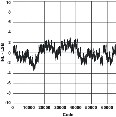 Figure 1. Integral Nonlinearity
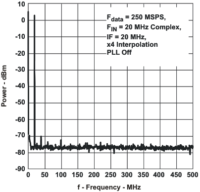 Figure 3. Single-Tone Spectral Plot
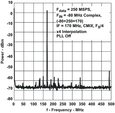 Figure 5. Single-Tone Spectral Plot
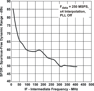 Figure 7. Out-Of-Band SFDR vs IF
 Figure 9. Two-Tone IMD vs Amplitude
 Figure 11. Two-Tone IMD Spectral Plot
 Figure 13. Single-Carrier W-CDMA Test Model 1
 Figure 15. Single-Carrier W-CDMA Test Model 1
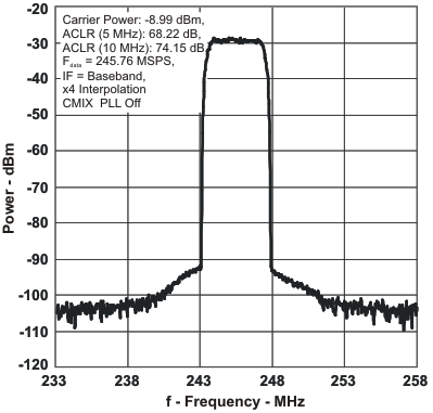 Figure 17. Single-Carrier W-CDMA Test Model 1
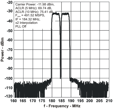 Figure 19. Two-Carrier W-CDMA Test Model 1
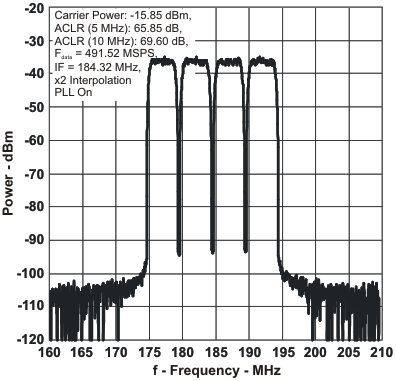 Figure 21. Four-Carrier W-CDMA Test Model 1
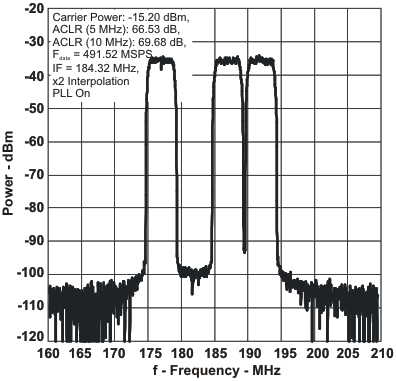 Figure 23. Three-Carrier W-CDMA Test Model 1 With Gap
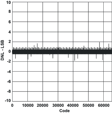 Figure 2. Differential Nonlinearity
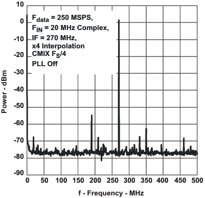 Figure 4. Single-Tone Spectral Plot
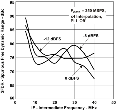
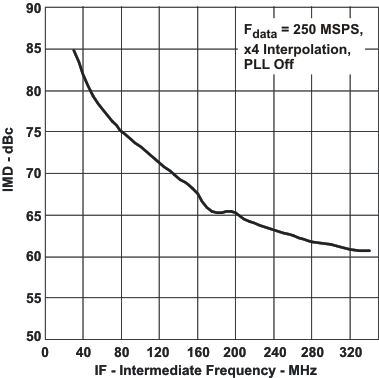 Figure 8. Two-Tone IMD vs Output Frequency
 Figure 10. Two-Tone IMD Spectral Plot
 Figure 12. Single-Carrier W-CDMA Test Model 1
 Figure 14. Single-Carrier W-CDMA Test Model 1
 Figure 16. Single-Carrier W-CDMA Test Model 1
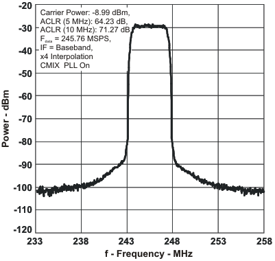 Figure 18. Single-Carrier W-CDMA Test Model 1
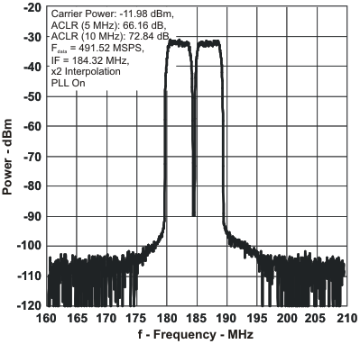 Figure 20. Two-Carrier W-CDMA Test Model 1
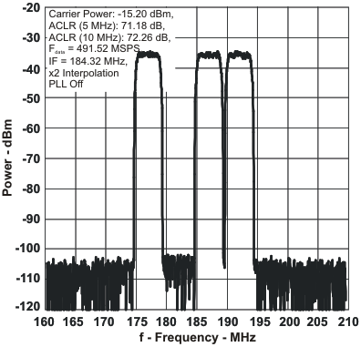 Figure 22. Three-Carrier W-CDMA Test Model 1 With Gap