SBAS438C May 2008 – November 2019 DAC9881
PRODUCTION DATA.
- 1 Features
- 2 Applications
- 3 Description
- 4 Revision History
- 5 Pin Configuration and Functions
-
6 Specifications
- 6.1 Absolute Maximum Ratings
- 6.2 ESD Ratings
- 6.3 Recommended Operating Conditions
- 6.4 Thermal Information
- 6.5 Electrical Characteristics: AVDD = 5 V
- 6.6 Electrical Characteristics: AVDD = 2.7 V
- 6.7 Timing Requirements—Standalone Operation Without SDO
- 6.8 Timing Requirements—Standalone Operation With SDO and Daisy-Chain Mode
- 6.9 Typical Characteristics: AVDD = 5 V
- 6.10 Typical Characteristics: AVDD = 2.7 V
-
7 Detailed Description
- 7.1 Overview
- 7.2 Functional Block Diagram
- 7.3 Feature Description
- 7.4 Device Functional Modes
- 8 Application and Implementation
- 9 Power Supply Recommendations
- 10Layout
- 11Device and Documentation Support
- 12Mechanical, Packaging, and Orderable Information
Package Options
Mechanical Data (Package|Pins)
- RGE|24
Thermal pad, mechanical data (Package|Pins)
- RGE|24
Orderable Information
7.1 Overview
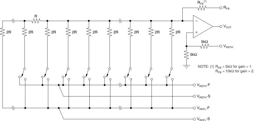
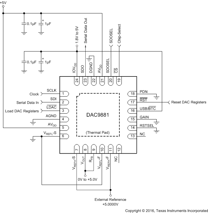
The DAC9881 is a single-channel, 18-bit, serial-input, voltage-output digital-to-analog converter (DAC). The architecture is an R-2R ladder configuration with the four MSBs segmented, followed by an operational amplifier that serves as a buffer, as shown in Figure 64. The on-chip output buffer allows rail-to-rail output swings while providing a low output impedance to drive loads. The DAC9881 operates from a single analog power supply that ranges from 2.7 V to 5.5 V, and typically consumes 850 μA when operating with a 5-V supply. Data are written to the device in a 24-bit word format, using an SPI serial interface. To enable compatibility with 1.8-V, 3-V, or 5-V logic families, an IOVDD supply pin is provided. This pin allows the DAC9881 input and output logic to be powered from the same logic supply used to interface signals to and from the device. Internal voltage translators are included in the DAC9881 to interface digital signals to the device core. See Figure 65 for the basic configuration of the DAC9881.
To provide a known power-up state, the DAC9881 is designed with a power-on reset function. Upon power-up, the DAC9881 is reset to either zero-scale or midscale depending on the state of the RSTSEL pin. A hardware reset can be performed by using the RST and RSTSEL pins.
 Figure 64. DAC9881 Architecture
  Figure 65. Basic Configuration