SBAS438C May 2008 – November 2019 DAC9881
PRODUCTION DATA.
- 1 Features
- 2 Applications
- 3 Description
- 4 Revision History
- 5 Pin Configuration and Functions
-
6 Specifications
- 6.1 Absolute Maximum Ratings
- 6.2 ESD Ratings
- 6.3 Recommended Operating Conditions
- 6.4 Thermal Information
- 6.5 Electrical Characteristics: AVDD = 5 V
- 6.6 Electrical Characteristics: AVDD = 2.7 V
- 6.7 Timing Requirements—Standalone Operation Without SDO
- 6.8 Timing Requirements—Standalone Operation With SDO and Daisy-Chain Mode
- 6.9 Typical Characteristics: AVDD = 5 V
- 6.10 Typical Characteristics: AVDD = 2.7 V
-
7 Detailed Description
- 7.1 Overview
- 7.2 Functional Block Diagram
- 7.3 Feature Description
- 7.4 Device Functional Modes
- 8 Application and Implementation
- 9 Power Supply Recommendations
- 10Layout
- 11Device and Documentation Support
- 12Mechanical, Packaging, and Orderable Information
Package Options
Mechanical Data (Package|Pins)
- RGE|24
Thermal pad, mechanical data (Package|Pins)
- RGE|24
Orderable Information
7.3.2 Reference Inputs
The reference high input, VREFH, can be set to any voltage in the range of 1.25 V to AVDD. The reference low input, VREFL, can be set to any voltage in the range of –0.2 V to +0.2 V (to provide a small offset to the output of the DAC9881, if desired). The current into VREFH and out of VREFL depends on the DAC code, and can vary from approximately 0.5 mA to 1 mA in the gain = 1X mode of operation. The reference high and low inputs appear as variable loads to the external reference circuit. If the external references can source or sink the required current, and if low impedance connections are made to the VREFH and VREFL pins, external reference buffers are not required. Figure 65 shows a simple configuration of the DAC9881 using external references without force and sense reference buffers.
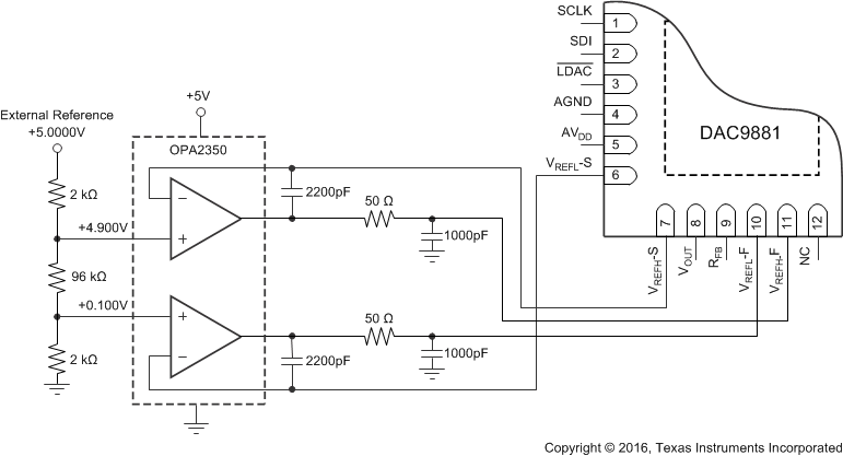
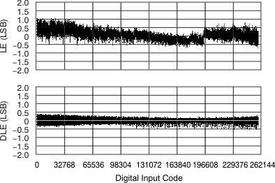
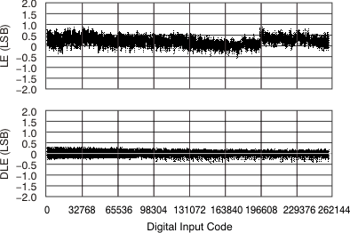
Kelvin sense connections for the reference high and low are included on the DAC9881. When properly used with external reference buffer op amps, these reference Kelvin sense pins make sure that the driven reference high and low voltages remain stable versus varying reference load currents. Figure 67 shows an example of a reference force and sense configuration of the DAC9881 operating from a single analog reference voltage. Both the VREFL and VREFH reference voltages are set to levels of 100 mV from the DAC9881 supply rails, and are derived from a 5-V external reference. Figure 68 illustrates the effect of not using the reference force and sense buffers to drive the DAC9881 VREFL and VREFH pins. Figure 69 shows the improvement when using the reference buffers. A slight degradation in INL and DNL performance is seen without the use of the force and sense buffer configuration.
 Figure 67. Buffered References (VREFH = +4.900 V and VREFL = 100 mV).
