DLPS136 November 2018 DLP650LNIR
PRODUCTION DATA.
- 1 Features
- 2 Applications
- 3 Description
- 4 Revision History
- 5 Pin Configuration and Functions
-
6 Specifications
- 6.1 Absolute Maximum Ratings
- 6.2 Storage Conditions
- 6.3 ESD Ratings
- 6.4 Recommended Operating Conditions
- 6.5 Thermal Information
- 6.6 Electrical Characteristics
- 6.7 Timing Requirements
- 6.8 System Mounting Interface Loads
- 6.9 Micromirror Array Physical Characteristics
- 6.10 Micromirror Array Optical Characteristics
- 6.11 Window Characteristics
- 6.12 Chipset Component Usage Specification
-
7 Detailed Description
- 7.1 Overview
- 7.2 System Functional Block Diagram
- 7.3
Feature Description
- 7.3.1 DLPC410: Digital Controller for DLP Discovery 4100 Chipset
- 7.3.2 DLPA200: DMD Micromirror Driver
- 7.3.3 DLPR410: PROM for DLP Discovery 4100 Chipset
- 7.3.4 DLP650LNIR: DLP 0.65 WXGA NIR 2xLVDS Series 450 DMD
- 7.3.5 Measurement Conditions
- 7.4 Device Operational Modes
- 7.5 Feature Description
- 7.6 Optical Interface and System Image Quality Considerations
- 7.7 Micromirror Temperature Calculations
- 7.8 Micromirror Landed-On/Landed-Off Duty Cycle
- 8 Application and Implementation
- 9 Power Supply Recommendations
- 10Layout
- 11Device and Documentation Support
- 12Mechanical, Packaging, and Orderable Information
Package Options
Mechanical Data (Package|Pins)
- FYL|149
Thermal pad, mechanical data (Package|Pins)
Orderable Information
6.7 Timing Requirements
Over Recommended Operating Conditions (unless otherwise noted).| PARAMETER DESCRIPTION | SIGNAL | MIN | TYP | MAX | UNIT | |
|---|---|---|---|---|---|---|
| LVDS(1) | ||||||
| tC | Clock Cycle Duration for DCLK_A | LVDS | 2.46 | ns | ||
| tC | Clock Cycle Duration for DCLK_B | LVDS | 2.46 | ns | ||
| tW | Pulse Duration for DCLK_A | LVDS | 1.07 | 1.23 | ns | |
| tW | Pulse Duration for DCLK_B | LVDS | 1.07 | 1.23 | ns | |
| tSU | Setup Time for D_A(15:0) before DCLK_A | LVDS | 0.35 | ns | ||
| tSU | Setup Time for D_A(15:0) before DCLK_B | LVDS | 0.35 | ns | ||
| tSU | Setup Time for SCTRL_A before DCLK_A | LVDS | 0.35 | ns | ||
| tSU | Setup Time for SCTRL_B before DCLK_B | LVDS | 0.35 | ns | ||
| tH | Hold time for D_A(15:0) after DCLK_A | LVDS | 0.50 | ns | ||
| tH | Hold time for D_B(15:0) after DCLK_B | LVDS | 0.50 | ns | ||
| tH | Hold Time for SCTRL_A after DCLK_A | LVDS | 0.50 | ns | ||
| tH | Hold Time for SCTRL_B after DCLK_B | LVDS | 0.50 | ns | ||
| tSKEW | Channel B relative to Channel A(2)(3) | LVDS | –1.23 | 1.23 | ns | |
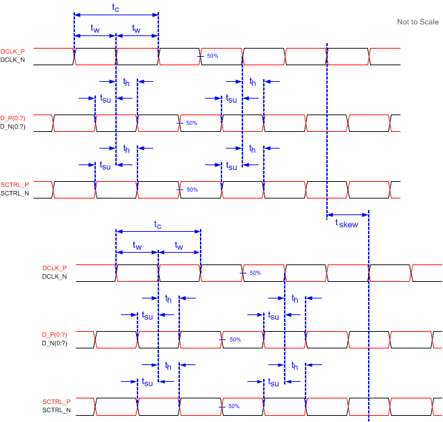
(1) See Figure 7 for timing requirements for LVDS.
(2) Channel A (Bus A) includes the following LVDS pairs: DCLK_AN and DCLK_AP, SCTRL_AN and SCTRL_AP, D_AN(15,13,11,9,7,5,3,1) and D_AP(15,13,11,9,7,5,3,1).
(3) Channel B (Bus B) includes the following LVDS pairs: DCLK_BN and DCLK_BP, SCTRL_BN and SCTRL_BP, D_BN(15,13,11,9,7,5,3,1) and D_BP(15,13,11,9,7,5,3,1).
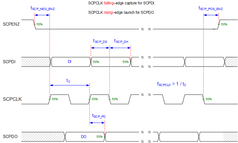
 Figure 3. SCP Timing Requirements
 See Recommended Operating Conditions for fSCPCLK, tSCP_DS, tSCP_DH, and tSCP_PD specifications.
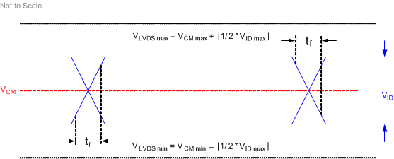
See Recommended Operating Conditions for tr and tf specifications and conditions.
 Figure 5. Test Load Circuit for Output Propagation Measurement
 For output timing analysis, the tester pin electronics and its transmission line effects must be taken into account. Use IBIS or other simulation tools to correlate the timing reference load to a system environment. See Figure 5.
 Figure 6. LVDS Waveform Requirements
 See Recommended Operating Conditions for VCM, VID, and VLVDS specifications and conditions.
 Figure 7. Timing Requirements
 See Timing Requirements for timing requirements and LVDS pairs per channel (bus) defining D_P(0:x) and D_N(0:x).
