DLPS194A November   2020  – June 2022 DLP670S

PRODUCTION DATA  

  1. Features
  2. Applications
  3. Description
  4. Revision History
  5. Pin Configuration and Functions
  6. Specifications
    1. 6.1  Absolute Maximum Ratings
    2. 6.2  Storage Conditions
    3. 6.3  ESD Ratings
    4. 6.4  Recommended Operating Conditions
    5. 6.5  Thermal Information
    6. 6.6  Electrical Characteristics
    7. 6.7  Capacitance at Recommended Operating Conditions
    8. 6.8  Timing Requirements
    9. 6.9  Typical Characteristics
    10. 6.10 System Mounting Interface Loads
    11. 6.11 Micromirror Array Physical Characteristics
    12. 6.12 Micromirror Array Optical Characteristics
    13. 6.13 Window Characteristics
    14. 6.14 Chipset Component Usage Specification
  7. Detailed Description
    1. 7.1 Overview
    2. 7.2 Functional Block Diagram
    3. 7.3 Feature Description
      1. 7.3.1 Power Interface
      2. 7.3.2 Timing
    4. 7.4 Device Functional Modes
    5. 7.5 Optical Interface and System Image Quality
      1. 7.5.1 Numerical Aperture and Stray Light Control
      2. 7.5.2 Pupil Match
      3. 7.5.3 Illumination Overfill
    6. 7.6 Micromirror Array Temperature Calculation
      1. 7.6.1 Micromirror Array Temperature Calculation using Illumination Power Density
      2. 7.6.2 Micromirror Array Temperature Calculation using Total Illumination Power
      3. 7.6.3 Micromirror Array Temperature Calculation using Screen Lumens
    7. 7.7 Micromirror Landed-On/Landed-Off Duty Cycle
      1. 7.7.1 Definition of Micromirror Landed-On/Landed-Off Duty Cycle
      2. 7.7.2 Landed Duty Cycle and Useful Life of the DMD
      3. 7.7.3 Landed Duty Cycle and Operational DMD Temperature
      4. 7.7.4 Estimating the Long-Term Average Landed Duty Cycle of a Product or Application
  8. Application and Implementation
    1. 8.1 Application Information
    2. 8.2 Typical Application
      1. 8.2.1 Design Requirements
      2. 8.2.2 Detailed Design Procedure
    3. 8.3 DMD Die Temperature Sensing
  9. Power Supply Recommendations
    1. 9.1 DMD Power Supply Power-Up Procedure
    2. 9.2 DMD Power Supply Power-Down Procedure
    3. 9.3 Restrictions on Hot Plugging and Hot Swapping
      1. 9.3.1 No Hot Plugging
      2. 9.3.2 No Hot Swapping
      3. 9.3.3 Intermittent or Voltage Power Spike Avoidance
  10. 10Layout
    1. 10.1 Layout Guidelines
      1. 10.1.1 Critical Signal Guidelines
      2. 10.1.2 Power Connection Guidelines
      3. 10.1.3 Noise Coupling Avoidance
    2. 10.2 Layout Example
      1. 10.2.1 Layers
      2. 10.2.2 Impedance Requirements
      3. 10.2.3 Trace Width, Spacing
        1. 10.2.3.1 Voltage Signals
  11. 11Device and Documentation Support
    1. 11.1 Third-Party Products Disclaimer
    2. 11.2 Device Support
      1. 11.2.1 Device Nomenclature
      2. 11.2.2 Device Markings
    3. 11.3 Documentation Support
      1. 11.3.1 Related Documentation
    4. 11.4 Receiving Notification of Documentation Updates
    5. 11.5 Support Resources
    6. 11.6 Trademarks
    7. 11.7 Electrostatic Discharge Caution
    8. 11.8 Glossary
  12. 12Mechanical, Packaging, and Orderable Information

Package Options

Mechanical Data (Package|Pins)
Thermal pad, mechanical data (Package|Pins)
Orderable Information

Description

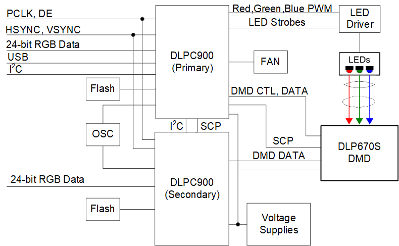
Featuring over 4.3 million micromirrors, the DLP670S digital micromirror device (DMD) is a spatial light modulator (SLM) that modulates the amplitude, direction, and phase of incoming light. This DMD coupled with its four 2xLVDS input data buses enables the display of high-resolution patterns at very fast pattern rates. The high resolution and fast pattern rates offered by the DLP670S make it well-suited to support a wide variety of industrial, medical, and advanced imaging applications. Reliable function and operation of the DLP670S is enabled in conjunction with dual DLPC900 digital controllers. This dedicated chipset provides flexible and easy-to-program patterns at the high pattern rates necessary to meet the requirements of a variety of end-equipment solutions.

The high resolution provides a direct benefit to the scanning of larger objects in 3D machine vision applications.

Get started with TI DLP® advanced light-control technology page to learn how to get started with the DLP670S. The DLP advanced light control resources on TI.com accelerate time to market, which include evaluation modules, reference designs,optical modules manufacturers, and DLP design network partners.

Table 3-1 Device Information
PART NUMBER PACKAGE BODY SIZE (NOM)
DLP670S(1) FYR (350) 35 mm × 32 mm
For all available packages, see the orderable addendum at the end of the data sheet.
GUID-20210304-CA0I-2DJG-ZSSX-0FVPPH6PSV3C-low.png DLP670S Simplified Schematic