DLPS048C March 2015 – June 2019 DLPC150
PRODUCTION DATA.
- 1 Features
- 2 Applications
- 3 Description
- 4 Revision History
- 5 Pin Configuration and Functions
-
6 Specifications
- 6.1 Absolute Maximum Ratings
- 6.2 ESD Ratings
- 6.3 Recommended Operating Conditions
- 6.4 Thermal Information
- 6.5 Electrical Characteristics Over Recommended Operating Conditions
- 6.6 Electrical Characteristics
- 6.7 High-Speed Sub-LVDS Electrical Characteristics
- 6.8 Low-Speed SDR Electrical Characteristics
- 6.9 System Oscillators Timing Requirements
- 6.10 Power-Up and Reset Timing Requirements
- 6.11 Parallel Interface Frame Timing Requirements
- 6.12 Parallel Interface General Timing Requirements
- 6.13 Flash Interface Timing Requirements
- 7 Parameter Measurement Information
- 8 Detailed Description
- 9 Application and Implementation
- 10Power Supply Recommendations
-
11Layout
- 11.1
Layout Guidelines
- 11.1.1 PCB Layout Guidelines For Internal Controller PLL Power
- 11.1.2 DLPC150 Reference Clock
- 11.1.3 General PCB Recommendations
- 11.1.4 General Handling Guidelines for Unused CMOS-Type Pins
- 11.1.5 Maximum Pin-to-Pin, PCB Interconnects Etch Lengths
- 11.1.6 Number of Layer Changes
- 11.1.7 Stubs
- 11.1.8 Terminations
- 11.1.9 Routing Vias
- 11.2 Layout Example
- 11.3 Thermal Considerations
- 11.1
Layout Guidelines
- 12Device and Documentation Support
- 13Mechanical, Packaging, and Orderable Information
Package Options
Mechanical Data (Package|Pins)
- ZEZ|201
Thermal pad, mechanical data (Package|Pins)
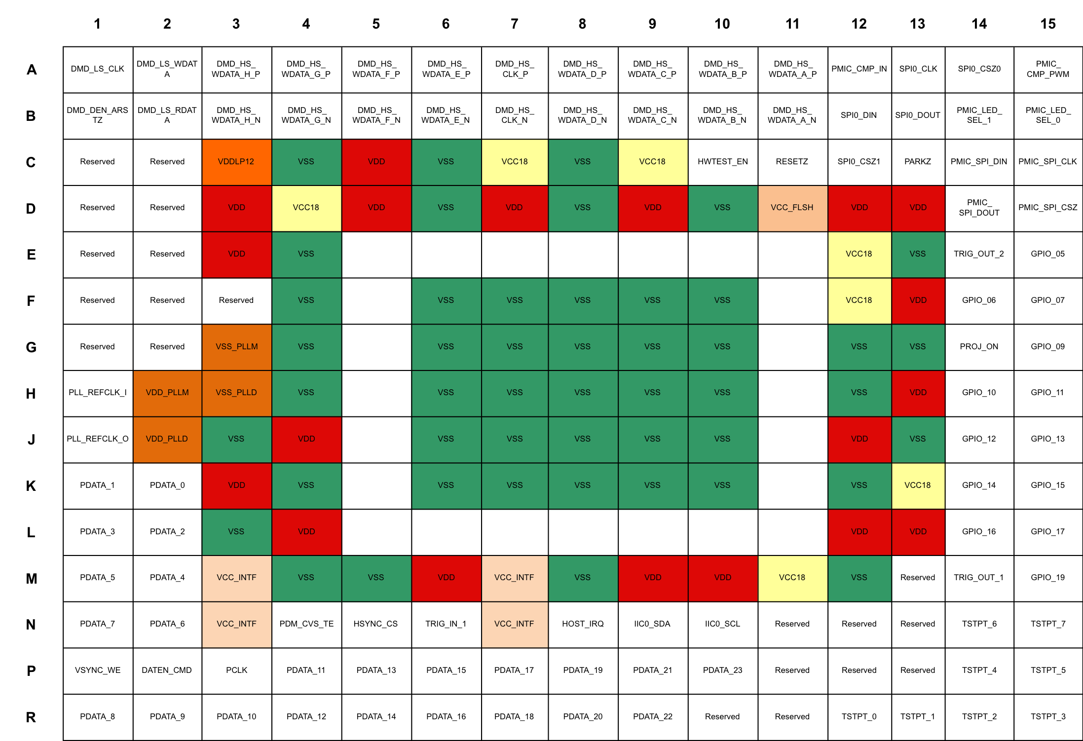
5.1 DLPC150 Mechanical Data
 Figure 1. 13- × 13-mm Package – VF Ball Grid Array
 Table 1. I/O Type Subscript Definition
| I/O TYPE | SUPPLY REFERENCE | ESD STRUCTURE | |
|---|---|---|---|
| SUBSCRIPT | DESCRIPTION | ||
| 1 | 1.8 LVCMOS I/O buffer with 8-mA drive | Vcc18 | ESD diode to GND and supply rail |
| 2 | 1.8 LVCMOS I/O buffer with 4-mA drive | Vcc18 | ESD diode to GND and supply rail |
| 3 | 1.8 LVCMOS I/O buffer with 24-mA drive | Vcc18 | ESD diode to GND and supply rail |
| 4 | 1.8 sub-LVDS output with 4-mA drive | Vcc18 | ESD diode to GND and supply rail |
| 5 | 1.8, 2.5, 3.3 LVCMOS with 4-mA drive | Vcc_INTF | ESD diode to GND and supply rail |
| 6 | 1.8 LVCMOS input | Vcc18 | ESD diode to GND and supply rail |
| 7 | 1.8-, 2.5-, 3.3-V I2C with 3-mA drive | Vcc_INTF | ESD diode to GND and supply rail |
| 8 | 1.8-V I2C with 3-mA drive | Vcc18 | ESD diode to GND and supply rail |
| 9 | 1.8-, 2.5-, 3.3-V LVCMOS with 8-mA drive | Vcc_INTF | ESD diode to GND and supply rail |
| 11 | 1.8, 2.5, 3.3 LVCMOS input | Vcc_INTF | ESD diode to GND and supply rail |
| 12 | 1.8-, 2.5-, 3.3-V LVCMOS input | Vcc_FLSH | ESD diode to GND and supply rail |
| 13 | 1.8-, 2.5-, 3.3-V LVCMOS with 8-mA drive | Vcc_FLSH | ESD diode to GND and supply rail |
Table 2. Internal Pullup and Pulldown Characteristics(1)(2)
| INTERNAL PULLUP AND PULLDOWN
RESISTOR CHARACTERISTICS |
VCCIO | MIN | MAX | UNIT |
|---|---|---|---|---|
| Weak pullup resistance | 3.3 V | 29 | 63 | kΩ |
| 2.5 V | 38 | 90 | kΩ | |
| 1.8 V | 56 | 148 | kΩ | |
| Weak pulldown resistance | 3.3 V | 30 | 72 | kΩ |
| 2.5 V | 36 | 101 | kΩ | |
| 1.8 V | 52 | 167 | kΩ |
(1) The resistance is dependent on the supply voltage level applied to the I/O.
(2) An external 8-kΩ pullup or pulldown (if needed) would work for any voltage condition to correctly pull enough to override any associated internal pullups or pulldowns.