DLPS048C March 2015 – June 2019 DLPC150
PRODUCTION DATA.
- 1 Features
- 2 Applications
- 3 Description
- 4 Revision History
- 5 Pin Configuration and Functions
-
6 Specifications
- 6.1 Absolute Maximum Ratings
- 6.2 ESD Ratings
- 6.3 Recommended Operating Conditions
- 6.4 Thermal Information
- 6.5 Electrical Characteristics Over Recommended Operating Conditions
- 6.6 Electrical Characteristics
- 6.7 High-Speed Sub-LVDS Electrical Characteristics
- 6.8 Low-Speed SDR Electrical Characteristics
- 6.9 System Oscillators Timing Requirements
- 6.10 Power-Up and Reset Timing Requirements
- 6.11 Parallel Interface Frame Timing Requirements
- 6.12 Parallel Interface General Timing Requirements
- 6.13 Flash Interface Timing Requirements
- 7 Parameter Measurement Information
- 8 Detailed Description
- 9 Application and Implementation
- 10Power Supply Recommendations
-
11Layout
- 11.1
Layout Guidelines
- 11.1.1 PCB Layout Guidelines For Internal Controller PLL Power
- 11.1.2 DLPC150 Reference Clock
- 11.1.3 General PCB Recommendations
- 11.1.4 General Handling Guidelines for Unused CMOS-Type Pins
- 11.1.5 Maximum Pin-to-Pin, PCB Interconnects Etch Lengths
- 11.1.6 Number of Layer Changes
- 11.1.7 Stubs
- 11.1.8 Terminations
- 11.1.9 Routing Vias
- 11.2 Layout Example
- 11.3 Thermal Considerations
- 11.1
Layout Guidelines
- 12Device and Documentation Support
- 13Mechanical, Packaging, and Orderable Information
Package Options
Mechanical Data (Package|Pins)
- ZEZ|201
Thermal pad, mechanical data (Package|Pins)
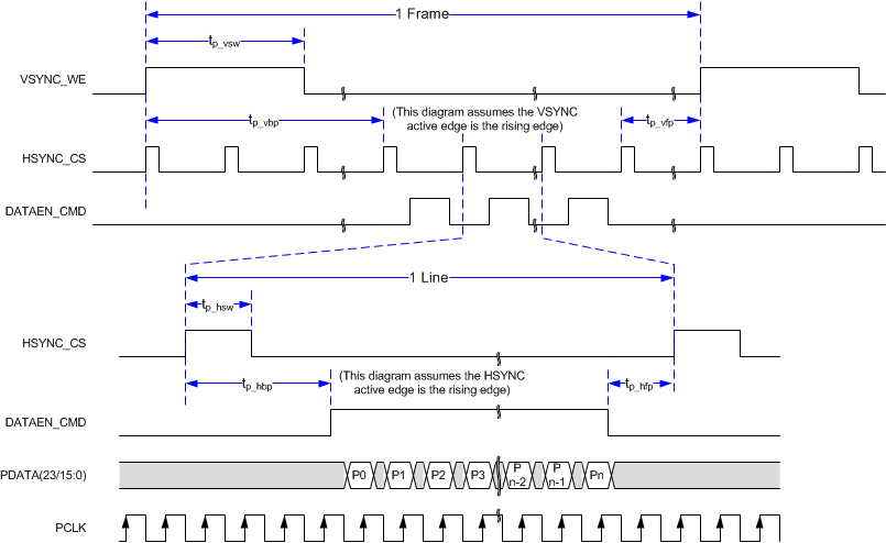
6.11 Parallel Interface Frame Timing Requirements
| MIN | MAX | UNIT | |||
|---|---|---|---|---|---|
| tp_vsw | Pulse duration – VSYNC_WE high | 50% reference points | 1 | lines | |
| tp_vbp | Vertical back porch (VBP) – time from the leading edge of VSYNC_WE to the leading edge HSYNC_CS for the first active line (see (2)) | 50% reference points | 2 | lines | |
| tp_vfp | Vertical front porch (VFP) – time from the leading edge of the HSYNC_CS following the last active line in a frame to the leading edge of VSYNC_WE (see (2)) | 50% reference points | 1 | lines | |
| tp_tvb | Total vertical blanking – time from the leading edge of HSYNC_CS following the last active line of one frame to the leading edge of HSYNC_CS for the first active line in the next frame. (This is equal to the sum of VBP (tp_vbp) + VFP (tp_vfp).) | 50% reference points | See (2) | lines | |
| tp_hsw | Pulse duration – HSYNC_CS high | 50% reference points | 4 | 128 | PCLKs |
| tp_hbp | Horizontal back porch – time from rising edge of HSYNC_CS to rising edge of DATAEN_CMD | 50% reference points | 4 | PCLKs | |
| tp_hfp | Horizontal front porch – time from falling edge of DATAEN_CMD to rising edge of HSYNC_CS | 50% reference points | 8 | PCLKs | |
| tp_thb | Total horizontal blanking – sum of horizontal front and back porches | 50% reference points | See (1) | PCLKs | |
(1) Total horizontal blanking is driven by the max line rate for a given source which will be a function of resolution and orientation. The following equation can be applied for this: tp_thb = Roundup[(1000 × ƒclock)/ LR] – APPL
where:
where:
- ƒclock = Pixel clock rate in MHz
- LR = Line rate in kHz
- APPL is the number of active pixels per (horizontal) line.
- If tp_thb is calculated to be less than tp_hbp + tp_hfp then the pixel clock rate is too low or the line rate is too high, and one or both must be adjusted.
(2) The minimum total vertical blanking is defined by the following equation: tp_tvb(min) = 6 + [6 × Max(1, Source_ALPF/ DMD_ALPF)] lines
where:
where:
- SOURCE_ALPF = Input source active lines per frame
- DMD_ALPF = Actual DMD used lines per frame supported
 Figure 5. Parallel Interface Frame Timing