DLPS023C January 2012 – August 2015 DLPC300
PRODUCTION DATA.
- 1 Features
- 2 Applications
- 3 Description
- 4 Revision History
- 5 Pin Configuration and Functions
-
6 Specifications
- 6.1 Absolute Maximum Ratings
- 6.2 ESD Ratings
- 6.3 Recommended Operating Conditions
- 6.4 Thermal Information
- 6.5 I/O Electrical Characteristics
- 6.6 Crystal Port Electrical Characteristics
- 6.7 Power Consumption
- 6.8 I2C Interface Timing Requirements
- 6.9 Parallel Interface Frame Timing Requirements
- 6.10 Parallel Interface General Timing Requirements
- 6.11 Parallel I/F Maximum Supported Horizontal Line Rate
- 6.12 BT.565 I/F General Timing Requirements
- 6.13 Flash Interface Timing Requirements
- 6.14 DMD Interface Timing Requirements
- 6.15 Mobile Dual Data Rate (mDDR) Memory Interface Timing Requirements
- 6.16 JTAG Interface: I/O Boundary Scan Application Switching Characteristics
- 7 Detailed Description
-
8 Application and Implementation
- 8.1 Application Information
- 8.2 Typical Application
- 8.3 System Examples
- 9 Power Supply Recommendations
-
10Layout
- 10.1
Layout Guidelines
- 10.1.1 Printed Circuit Board Design Guidelines
- 10.1.2 Printed Circuit Board Layer Stackup Geometry
- 10.1.3 Signal Layers
- 10.1.4 Routing Constraints
- 10.1.5 Termination Requirements
- 10.1.6 PLL
- 10.1.7 General Handling Guidelines for Unused CMOS-Type Pins
- 10.1.8 Hot-Plug Usage
- 10.1.9 External Clock Input Crystal Oscillator
- 10.2 Layout Example
- 10.3 Thermal Considerations
- 10.1
Layout Guidelines
- 11Device and Documentation Support
- 12Mechanical, Packaging, and Orderable Information
Package Options
Refer to the PDF data sheet for device specific package drawings
Mechanical Data (Package|Pins)
- ZVB|176
Thermal pad, mechanical data (Package|Pins)
Orderable Information
10 Layout
10.1 Layout Guidelines
10.1.1 Printed Circuit Board Design Guidelines
The PCB design may vary depending on system design. Table 14 provides general recommendations on the PCB design.
Table 14. PCB General Recommendations for MDDR and DMD Interfaces
| DESCRIPTION | RECOMMENDATION |
|---|---|
| Configuration | Asymmetric dual stripline |
| Etch thickness (T) | 0.5-oz. (0.18-mm thick) copper |
| Single-ended signal impedance | 50 Ω (± 10%) |
| Differential signal impedance | 100 Ω differential (± 10%) |
10.1.2 Printed Circuit Board Layer Stackup Geometry
The PCB layer stack may vary depending on system design. However, careful attention is required in order to meet design considerations listed in the following sections. Table 15 provides general guidelines for the mDDR and DMD interface stackup geometry.
Table 15. PCB Layer Stackup Geometry for MDDR and DMD Interfaces
| PARAMETER | DESCRIPTION | RECOMMENDATION |
|---|---|---|
| Reference plane 1 | Ground plane for proper return | |
| Er | Dielectirc FR4 | 4.2 (nominal) |
| H1 | Signal trace distance to reference plane 1 | 5 mil (0.127 mm) |
| H2 | Signal trace distance to reference plane 2 | 34.2 mil (0.869 mm) |
| Reference plane 2 | I/O power plane or ground |
10.1.3 Signal Layers
The PCB signal layers should follow these recommendations:
- Layer changes should be minimized for single-ended signals.
- Individual differential pairs can be routed on different layers, but the signals of a given pair should not change layers.
- Stubs should be avoided.
- Only voltage or low-frequency signals should be routed on the outer layers, except as noted previously in this document.
- Double data rate signals should be routed first.
10.1.4 Routing Constraints
In order to meet the specifications listed in Table 16 and Table 17, typically the PCB designer must route these signals manually (not using automated PCB routing software). In case of length matching requirements, the longer signals should be routed in a serpentine fashion, keeping the number of turns to a minimum and the turn angles no sharper than 45 degrees. Avoid routing long traces all around the PCB.
Table 16. Signal Length Routing Constraints for MDDR and DMD Interfaces
| SIGNALS | MAX SIGNAL SINGLE-BOARD ROUTING LENGTH | MAX SIGNAL MULTI-BOARD ROUTING LENGTH |
|---|---|---|
| DMD_D(14:0), DMD_CLK, DMD_TRC, DMD_SCTRL, DMD_LOADB, DMD_OE, DMD_DRC_STRB, DMD_DRC_BUS, DMD_SAC_CLK, and DMD_SAC_BUS | 4 in (10.15 cm) | 3.5 in (8.8891 cm) |
| MEM_CLK_P, MEM_CLK_N, MEM_A(12:0), MEM_BA(1:0), MEM_CKE, MEM_CS, MEM_RAS, MEM_CAS, and MEM_WE | 2.5 in (6.35 cm) | Not recommended |
| MEM_DQ(15:0), MEM_LDM, MEM_UDM, MEM_LDQS, MEM_UDQS | 1.5 in (3.81 cm) | Not recommended |
Each high-speed, single-ended signal must be routed in relation to its reference signal, such that a constant impedance is maintained throughout the routed trace. Avoid sharp turns and layer switching while keeping lengths to a minimum. The following signals should follow these signal matching requirements.
Table 17. High-Speed Signal Matching Requirements for MDDR and DMD Interfaces
| SIGNALS | REFERENCE SIGNAL | MAX MISMATCH | UNIT |
|---|---|---|---|
| DMD_D(14:0), DMD_TRC, DMD_SCTRL, DMD_LOADB, DMD_OE, | DMD_DCLK | ±500 (12.7) | mil (mm) |
| DMD_DRC_STRB, DMD_DRC_BUS | DMD_DCLK | ±750 (19.05) | mil (mm) |
| DMD_SAC_CLK | DMD_DCLK | ±500 (12.7) | mil (mm) |
| DMD_SAC_BUS | DMD_SAC_CLK | ±750 (19.05) | mil (mm) |
| MEM_CLK_P | MEM_CLK_N | ±150 (3.81) | mil (mm) |
| MEM_DQ(7:0), MEM_LDM | MEM_LDQS | ±300 (7.62) | mil (mm) |
| MEM_DQ(15:8), MEM_UDM | MEM_UDQS | ±300 (7.62) | mil (mm) |
| MEM_A(12:0), MEM_BA(1:0), MEM_CKE, MEM_CS, MEM_RAS, MEM_CAS, MEM_WE | MEM_CLK_P, MEM_CLK_N | ±1000 (25.4) | mil (mm) |
| MEM_LDQS, MEM_UDQS | MEM_CLK_P, MEM_CLK_N | ±300 (7.62) | mil (mm) |
10.1.5 Termination Requirements
Table 18 lists the termination requirements for the DMD and mDDR interfaces.
For applications where the routed distance of the mDDR or DMD signal can be kept less than 0.75 inches, then this signal is short enough not to be considered a transmission line and should not need a series terminating resistor.
Table 18. Termination Requirements for MDDR and DMD Interfaces
| SIGNALS | SYSTEM TERMINATION |
|---|---|
| DMD_D(14:0), DMD_CLK, DMD_TRC, DMD_SCTRL, DMD_LOADB, DMD_DRC_STRB, DMD_DRC_BUS, DMD_SAC_CLK, and DMD_SAC_BUS | Terminated at source with 10-Ω to 30-Ω series resistor. 30 Ω is recommended for most applications as this minimizes over/under-shoot and reduces EMI. |
| MEM_CLK_P and MEM_CLK_N | Terminated at source with 30-Ω series resistor. The pair should also be terminated with an external 100-Ω differential termination across the two signals as close to the mDDR as possible. |
| MEM_DQ(15:0), MEM_LDM, MEM_UDM, MEM_LDQS, MEM_UDQS | Terminated with 30-Ω series resistor located midway between the two devices |
| MEM_A(12:0), MEM_BA(1:0), MEM_CKE, MEM_CS, MEM_RAS, MEM_CAS, and MEM_WE | Terminated at the source with a 30-Ω series resistor |
Spacer
10.1.6 PLL
The DLPC300 contains one internal PLL that has a dedicated analog supply (VDD_PLL, VSS_PLL). As a minimum, the VDD_PLL power and VSS_PLL ground pins should be isolated using an RC-filter consisting of two 50-Ω series ferrites and two shunt capacitors (to widen the spectrum of noise absorption). TI recommends that one capacitor be a 0.1-µF capacitor and the other be a 0.01-µF capacitor. All four components should be placed as close to the controller as possible, but it is especially important to keep the leads of the high-frequency capacitors as short as possible. Note that both capacitors should be connected across VDD_PLL and VSS_PLL on the controller side of the ferrites.
The PCB layout is critical to PLL performance. It is vital that the quiet ground and power are treated like analog signals. Therefore, VDD_PLL must be a single trace from the DLPC300 to both capacitors and then through the series ferrites to the power source. The power and ground traces should be as short as possible, parallel to each other and as close as possible to each other. See Figure 20.
10.1.7 General Handling Guidelines for Unused CMOS-Type Pins
To avoid potentially damaging current caused by floating CMOS input-only pins, TI recommends that unused controller input pins be tied through a pullup resistor to its associated power supply or through a pulldown to ground. For controller inputs with internal pullup or pulldown resistors, it is unnecessary to add an external pullup/pulldown unless specifically recommended. Note that internal pullup and pulldown resistors are weak and should not be expected to drive the external line. The DLPC300 implements very few internal resistors and these are noted in the pin list.
Unused output-only pins can be left open.
When possible, TI recommends that unused bidirectional I/O pins be configured to their output state such that the pin can be left open. If this control is not available and the pins may become an input, then they should be pulled up (or pulled down) using an appropriate resistor.
10.1.8 Hot-Plug Usage
Note that the DLPC300 provides fail-safe I/O on all host-interface signals (signals powered by VCC_INTF). This allows these inputs to be driven high even when no I/O power is applied. Under this condition, the DLPC300 does not load the input signal nor draw excessive current that could degrade controller reliability. Thus, for example, the I2C bus from the host to other components would not be affected by powering off VCC_INTF to the DLPC300. Note that TI recommends weak pullups or pulldowns on signals feeding back to the host to avoid floating inputs.
10.1.9 External Clock Input Crystal Oscillator
The DLPC300 requires an external reference clock to feed its internal PLL. This reference may be supplied via a crystal or oscillator. The DLPC300 accepts a reference clock of 16.667 MHz with a maximum frequency variation of 200 ppm (including aging, temperature, and trim component variation). When a crystal is used, several discrete components are also required as shown in Figure 19.
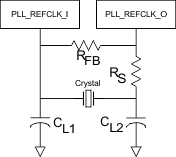
- Cstray_pll_refclk_i = Sum of package and PCB stray capacitance at the crystal pin associated with the ASIC pin pll_refclk_i.
- Cstray_pll_refclk_o = Sum of package and PCB stray capacitance at the crystal pin associated with the ASIC pin pll_refclk_o.
If an external oscillator is used, then the oscillator output must drive the PLL_REFCLK_I pin on the DLPC300 controller, and the PLL_REFCLK_O pins should be left unconnected. The benefit of an oscillator is that it can be made to provide a spread-spectrum clock that reduces EMI. However, the DLPC300 can only accept between 0% to –2% spreading (that is, down spreading only) with a modulation frequency between 20 and 65 kHz and a triangular waveform.
Similar to the crystal option, the oscillator input frequency is limited to 16.667 MHz.
It is assumed that the external crystal or oscillator stabilizes within 50 ms after stable power is applied.
Table 19 contains the recommended crystal configuration parameters.
Table 19. Recommended Crystal Configuration
| PARAMETER | RECOMMENDED | UNIT |
|---|---|---|
| Crystal circuit configuration | Parallel resonant | |
| Crystal type | Fundamental (first harmonic) | |
| Crystal nominal frequency | 16.667 | MHz |
| Crystal frequency tolerance (including accuracy, temperature, aging, and trim sensitivity) | ±200 | PPM |
| Crystal drive level | 100 max | uW |
| Crystal equivalent series resistance (ESR) | 80 max | Ω |
| Crystal load | 12 | pF |
| RS drive resistor (nominal) | 100 | Ω |
| RFB feedback resistor (nominal) | 1 | MΩ |
| CL1 external crystal load capacitor | See Figure 19 | pF |
| CL2 external crystal load capacitor | See Figure 19 | pF |
| PCB layout | A ground isolation ring around the crystal is recommended |
10.2 Layout Example
A complete schematic and layout example is provided in the DLP 0.3 WVGA Chipset Reference Design, which is implemented in the DLP LightCrafter EVM. The PCB stack up for this design can be seen in Table 20.
Table 20. Driver Board PCB Stackup and Impedance(1)
| Layer | Material Type | Thickness (mil) | Refer Layer | Impedance | |
|---|---|---|---|---|---|
| 50 Ω (Single End) | 100 Ω (Differential Pair) | ||||
| SolderMask | 0.80 | ||||
| Add Plating | 1.04 | ||||
| L1 - Top | L1 | 0.46 | L2 | 5.5 mil (50.4 Ω) | 4 mil /6 mil spacing /4 mil (99.1 Ω) |
| Prepreg | 3.49 | ||||
| L2 - GND | L2 | 1.10 | |||
| Prepreg | 3.39 | ||||
| L3 - Signal | L3 | 1.10 | L2/L4 | 3.5 mil (49.5 Ω) | |
| Prepreg | 5.32 | ||||
| L4 - GND | L4 | 0.70 | |||
| Core | 12 | ||||
| L5 - PWR | L5 | 0.70 | |||
| Prepreg | 5.27 | ||||
| L6 - Signal | L6 | 1.10 | L5/L7 | 3.5 mil (49.5 Ω) | |
| Prepreg | 3.45 | ||||
| L7 - GND | L7 | 1.10 | |||
| Prepreg | 3.5 | ||||
| L8 - Bottom | L8 | 0.46 | L7 | 5.5 mil (50.4 Ω) | 4 mil /6 mil spacing /4 mil (99.1 Ω) |
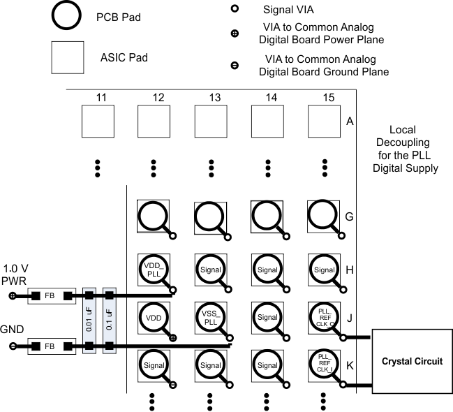 Figure 20. PLL Filter Layout
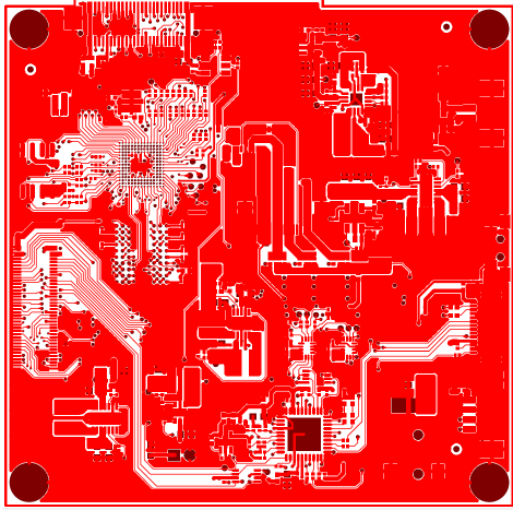 Figure 21. Top Board Layer
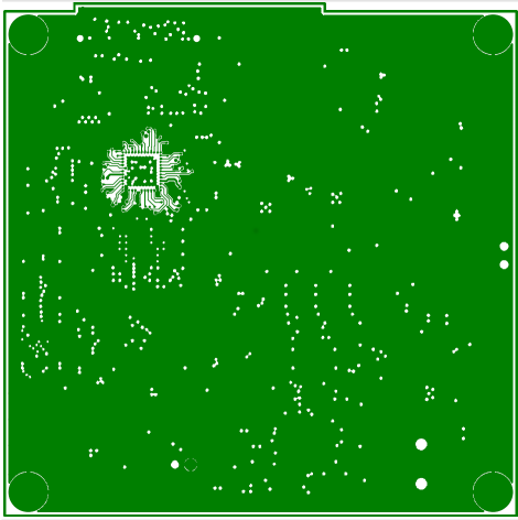 Figure 22. Internal Layer
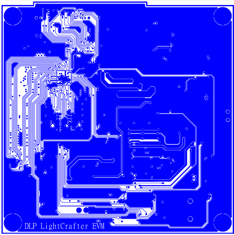 Figure 23. Bottom Board Layer
10.3 Thermal Considerations
The underlying thermal limitation for the DLPC300 is that the maximum operating junction temperature (TJ) not be exceeded (see Recommended Operating Conditions). This temperature depends on operating ambient temperature, airflow, PCB design (including the component layout density and the amount of copper used), power dissipation of the DLPC300, and power dissipation of surrounding components. The DLPC300 package is designed primarily to extract heat through the power and ground planes of the PCB. Thus, copper content and airflow over the PCB are important factors.