DLPS156F January 2019 – November 2024 DLPC3436
PRODUCTION DATA
- 1
- 1 Features
- 2 Applications
- 3 Description
- 4 Pin Configuration and Functions
-
5 Specifications
- 5.1 Absolute Maximum Ratings
- 5.2 ESD Ratings
- 5.3 Recommended Operating Conditions
- 5.4 Thermal Information
- 5.5 Power Electrical Characteristics
- 5.6 Pin Electrical Characteristics
- 5.7 Internal Pullup and Pulldown Electrical Characteristics
- 5.8 DMD SubLVDS Interface Electrical Characteristics
- 5.9 DMD Low-Speed Interface Electrical Characteristics
- 5.10 System Oscillator Timing Requirements
- 5.11 Power Supply and Reset Timing Requirements
- 5.12 Parallel Interface Frame Timing Requirements
- 5.13 Parallel Interface General Timing Requirements
- 5.14 Flash Interface Timing Requirements
- 5.15 Other Timing Requirements
- 5.16 DMD SubLVDS Interface Switching Characteristics
- 5.17 DMD Parking Switching Characteristics
- 5.18 Chipset Component Usage Specification
-
6 Detailed Description
- 6.1 Overview
- 6.2 Functional Block Diagram
- 6.3 Feature Description
- 6.4 Device Functional Modes
- 6.5 Programming
- 7 Application and Implementation
- 8 Power Supply Recommendations
- 9 Layout
- 10Device and Documentation Support
- 11Revision History
- 12Mechanical, Packaging, and Orderable Information
Package Options
Mechanical Data (Package|Pins)
- ZVB|176
Thermal pad, mechanical data (Package|Pins)
Orderable Information
8.2 System Power-Up and Power-Down Sequence
Although the DLPC34x6 requires an array of power supply voltages, (for example, VDD, VDDLP12, VDD_PLLM/D, VCC18, VCC_FLSH, VCC_INTF), because VDDLP12 is tied to the 1.1V VDD supply, then there are no restrictions regarding the relative order of power supply sequencing to avoid damaging the controller (This is true for both power-up and power-down scenarios). Similarly, there is no minimum time between powering-up or powering-down the different supplies if VDDLP12 is tied to the 1.1V VDD supply.
Although there is no risk of damaging the controller if the above power sequencing rules are followed, consider the following additional power sequencing recommendations for proper system operation.
- So that DLPC34x6 output signal states behave as expected, all controller I/O supplies should remain applied while VDD core power is applied. If VDD core power is removed while the I/O supply (VCC_INTF) is applied, then the output signal state associated with the inactive I/O supply goes to a high impedance state.
- Additional power sequencing rules may exist for devices that share the supplies with the controller, and thus these devices may force additional system power sequencing requirements.
Note that when VDD core power is applied, but I/O power is not applied, additional leakage current may be drawn. This added leakage does not affect normal controller operation or reliability.
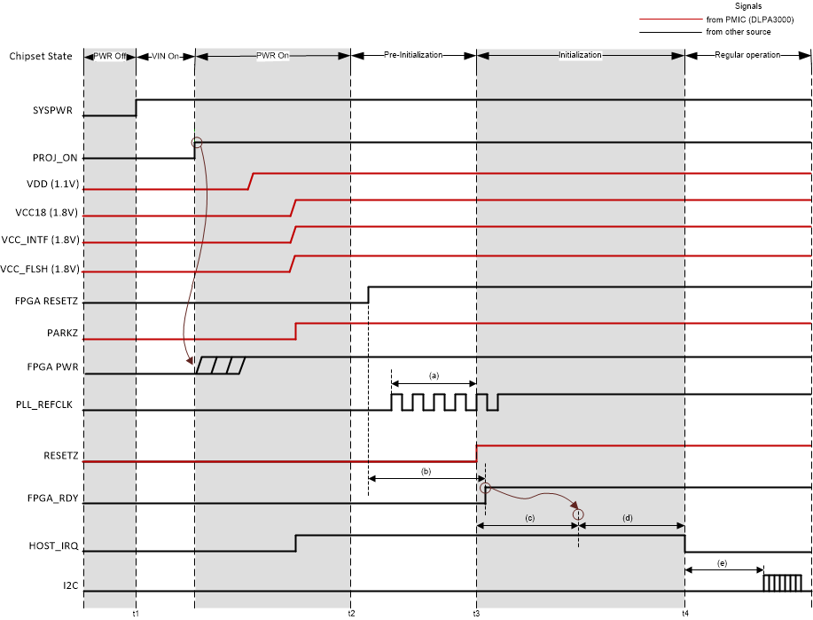
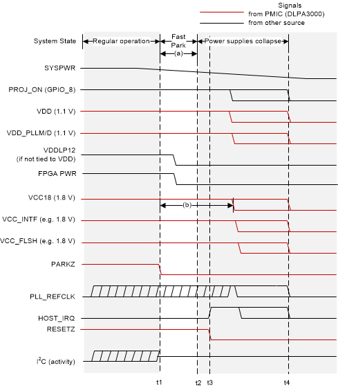
Figure 8-1, Figure 8-2, and Figure 8-3 show the controller power-up and power-down sequence for both the normal PARK and fast PARK operations of the DLPC34x6 controller.
During a normal park, maintain SYSPWR within specification for at least 50ms after PROJ_ON goes low. This is to allow the DMD to be parked and the power supply rails to safely power down. After 50ms, SYSPWR can be turned off. If a DLPA200x is used, it is also recommended that the 1.8V supply fed into the DLPA200x load switch be maintained within specification for at least 50ms after PROJ_ON goes low.

| t1: | SYSPWR (VIN) applied to the PMIC. All other voltage rails are derived from SYSPWR. |
| t2: | All supplies reach 95% of their specified nominal value. Note HOST_IRQ may go high sooner if it is pulled up to a different external supply. |
| t3: | Point where RESETZ is deasserted (goes high). This indicates the beginning of the controller auto-initialization routine. |
| t4: | HOST_IRQ goes low to indicate initialization is complete. I2C is now ready to accept commands. |
| (a): | The typical delay between the PLL reference clock becoming active and RESETZ being deasserted (going high) is less than 1ms. PLL_REFCLK must be stable within 5ms of all power being applied, and may be active before power is applied. |
| (b): | There is a typical delay of 1.5s between being FPGA RESETZ being deasserted and FPGA_RDY being asserted (going high). This duration is due to FPGA boot logic. |
| (c): | There is a typical controller boot time of 100ms. PARKZ must be high before RESETZ releases to support auto-initialization. RESETZ must also be held low for at least 5ms after the power supplies are in specification. |
| (d): | There is a typical FPGA setup time of 2.75ms before the system completes boot process. During this period, the DLPC34x6 controller writes startup values to the FPGA registers. |
| (e): | After FPGA setup is complete, I2C now accepts commands. |

| t1: | PROJ_ON goes low to begin the power down sequence. |
| t2: | The controller finishes parking the DMD. |
| t3: | Controller power supplies are turned off. |
| (a): | The DMD will be parked within 20ms of PROJ_ON being deasserted (going low). VDD, VDD_PLLM/D, VCC18, VCC_INITF, and VCC_FLSH power supplies and the PLL_REFCLK must be held within specification for a minimum of 20ms after PROJ_ON is deasserted (goes low). However, 20ms does not satisfy the typical shutdown timing of the entire chipset. It is therefore recommended to follow note (c). |
| (b): | DMD reset voltage regulation stops typically after 12ms of normal DMD park being completed. |
| (c): | It is recommended that SYSPWR not be turned off for 50ms after PROJ_ON is deasserted (goes low). This time allows the DMD to be parked, the controller to turn off, and the PMIC supplies to shut down. |

| t1: | A fault is detected and PARKZ is asserted (goes low) to tell the controller to initiate a fast park of the DMD. |
| t2: | The controller finishes the fast park procedure. |
| t3: | Eventually all power supplies that were derived from SYSPWR collapse. |
| t4: | System is completely turned off. |
| (a): | VDD, VDD_PLLM/D, VCC18, VCC_INITF, and VCC_FLSH power supplies and the PLL_REFCLK must be held within specification for a minimum of 32µs after PARKZ is asserted (goes low). |
| (b): | VCC18 must remain in specification long enough to satisfy DMD power sequencing requirements defined in the DMD data sheet. Also see the DLPAxxxx data sheets for more information. |