SLVSG22B January 2023 – March 2024 DRV8145-Q1
PRODUCTION DATA
- 1
- 1 Features
- 2 Applications
- 3 Description
- 4 Device Comparison
- 5 Pin Configuration and Functions
-
6 Specifications
- 6.1 Absolute Maximum Ratings
- 6.2 ESD Ratings
- 6.3 Recommended Operating Conditions
- 6.4 Thermal Information
- 6.5
Electrical Characteristics
- 6.5.1 Power Supply & Initialization
- 6.5.2 Logic I/Os
- 6.5.3 SPI I/Os
- 6.5.4 Configuration Pins - HW Variant Only
- 6.5.5 Power FET Parameters
- 6.5.6 Switching Parameters with High-Side Recirculation
- 6.5.7 Switching Parameters with Low-Side Recirculation
- 6.5.8 IPROPI & ITRIP Regulation
- 6.5.9 Over Current Protection (OCP)
- 6.5.10 Over Temperature Protection (TSD)
- 6.5.11 Voltage Monitoring
- 6.5.12 Load Monitoring
- 6.5.13 Fault Retry Setting
- 6.5.14 Transient Thermal Impedance & Current Capability
- 6.6 SPI Timing Requirements
- 6.7 Switching Waveforms
- 6.8 Typical Characteristics
-
7 Detailed Description
- 7.1 Overview
- 7.2 Functional Block Diagram
- 7.3
Feature Description
- 7.3.1 External Components
- 7.3.2 Bridge Control
- 7.3.3 Device Configuration
- 7.3.4
Protection and Diagnostics
- 7.3.4.1 Over Current Protection (OCP)
- 7.3.4.2 Over Temperature Protection (TSD)
- 7.3.4.3 Off-State Diagnostics (OLP)
- 7.3.4.4 On-State Diagnostics (OLA) - SPI Variant Only
- 7.3.4.5 VM Over Voltage Monitor
- 7.3.4.6 VM Under Voltage Monitor
- 7.3.4.7 Charge pump under voltage monitor
- 7.3.4.8 Power On Reset (POR)
- 7.3.4.9 Event Priority
- 7.4 Programming - SPI Variant Only
- 8 Register Map - SPI Variant Only
- 9 Application and Implementation
- 10Device and Documentation Support
- 11Revision History
- 12Mechanical, Packaging, and Orderable Information
Package Options
Mechanical Data (Package|Pins)
Thermal pad, mechanical data (Package|Pins)
- PWP|28
Orderable Information
9.4.2 Layout Example
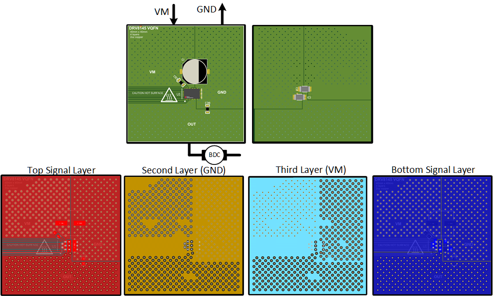
The following figure shows a layout example for a 4cm X 4cm x 1.6mm, 4 layer PCB for a leaded package device. The 4 layers uses 2oz copper on top/ bottom signal layers and 1oz copper on internal supply layers, with 0.3mm thermal via drill diameter, 0.025mm Cu plating, 1mm minimum via pitch. The same layout can be adopted for the non-leaded VQFN-HR package as well. The Section 6.5.14 for the 4cm X 4cm X 1.6mm is based on a similar layout.
Note: The layout example shown is for a full-bridge topology using DRV814xQ1 device in VQFN-HR package.
 Figure 9-8 Layout example: 4cm x 4 cm x 1.6mm, 4 layer PCB