SLOSE98A December 2022 – September 2023 DRV8461
PRODUCTION DATA
- 1
- 1 Features
- 2 Applications
- 3 Description
- 4 Revision History
- 5 Pin Configuration and Functions
- 6 Specifications
-
7 Detailed Description
- 7.1 Overview
- 7.2 Functional Block Diagram
- 7.3
Feature Description
- 7.3.1 Interface of Operation
- 7.3.2 Stepper Motor Driver Current Ratings
- 7.3.3 PWM Motor Drivers
- 7.3.4 Microstepping Indexer
- 7.3.5 Indexer Output
- 7.3.6 Automatic Microstepping Mode
- 7.3.7 Custom Microstepping Table
- 7.3.8 Current Regulation
- 7.3.9 Standstill Power Saving Mode
- 7.3.10 Current Regulation Decay Modes
- 7.3.11 Current Sensing with External Resistor
- 7.3.12 Silent step decay mode
- 7.3.13 Auto-torque Dynamic Current Adjustment
- 7.3.14 Charge Pump
- 7.3.15 Linear Voltage Regulator
- 7.3.16 VCC Voltage Supply
- 7.3.17 Logic Level, Tri-Level and Quad-Level Pin Diagrams
- 7.3.18 Spread Spectrum
- 7.3.19
Protection Circuits
- 7.3.19.1 VM Undervoltage Lockout
- 7.3.19.2 VCP Undervoltage Lockout (CPUV)
- 7.3.19.3 Logic Supply Power on Reset (POR)
- 7.3.19.4 Overcurrent Protection (OCP)
- 7.3.19.5 Stall Detection
- 7.3.19.6 Open-Load Detection (OL)
- 7.3.19.7 Overtemperature Warning (OTW)
- 7.3.19.8 Thermal Shutdown (OTSD)
- 7.3.19.9 Supply voltage sensing
- 7.3.19.10 nFAULT Output
- 7.3.19.11 Fault Condition Summary
- 7.3.20 Device Functional Modes
- 7.4 Programming
- 7.5
Register Maps
- 7.5.1 Status Registers
- 7.5.2
Control Registers
- 7.5.2.1 CTRL1 (address = 0x04) [Default = 0Fh]
- 7.5.2.2 CTRL2 (address = 0x05) [Default = 06h]
- 7.5.2.3 CTRL3 (address = 0x06) [Default = 38h]
- 7.5.2.4 CTRL4 (address = 0x07) [Default = 49h]
- 7.5.2.5 CTRL5 (address = 0x08) [Default = 03h]
- 7.5.2.6 CTRL6 (address = 0x09) [Default = 20h]
- 7.5.2.7 CTRL7 (address = 0x0A) [Default = FFh]
- 7.5.2.8 CTRL8 (address = 0x0B) [Default = 0Fh]
- 7.5.2.9 CTRL9 (address = 0x0C) [Default = 10h]
- 7.5.2.10 CTRL10 (address = 0x0D) [Default = 80h]
- 7.5.2.11 CTRL11 (address = 0x0E) [Default = FFh]
- 7.5.2.12 CTRL12 (address = 0x0F) [Default = 20h]
- 7.5.2.13 CTRL13 (address = 0x10) [Default = 10h]
- 7.5.2.14 CTRL14 (address = 0x3C) [Default = 58h]
- 7.5.3 Indexer Registers
- 7.5.4
Custom Microstepping Registers
- 7.5.4.1 CUSTOM_CTRL1 (address = 0x16) [Default = 00h]
- 7.5.4.2 CUSTOM_CTRL2 (address = 0x17) [Default = 00h]
- 7.5.4.3 CUSTOM_CTRL3 (address = 0x18) [Default = 00h]
- 7.5.4.4 CUSTOM_CTRL4 (address = 0x19) [Default = 00h]
- 7.5.4.5 CUSTOM_CTRL5 (address = 0x1A) [Default = 00h]
- 7.5.4.6 CUSTOM_CTRL6 (address = 0x1B) [Default = 00h]
- 7.5.4.7 CUSTOM_CTRL7 (address = 0x1C) [Default = 00h]
- 7.5.4.8 CUSTOM_CTRL8 (address = 0x1D) [Default = 00h]
- 7.5.4.9 CUSTOM_CTRL9 (address = 0x1E) [Default = 00h]
- 7.5.5
Auto torque Registers
- 7.5.5.1 ATQ_CTRL1 (address = 0x1F) [Default = 00h]
- 7.5.5.2 ATQ_CTRL2 (address = 0x20) [Default = 00h]
- 7.5.5.3 ATQ_CTRL3 (address = 0x21) [Default = 00h]
- 7.5.5.4 ATQ_CTRL4 (address = 0x22) [Default = 20h]
- 7.5.5.5 ATQ_CTRL5 (address = 0x23) [Default = 00h]
- 7.5.5.6 ATQ_CTRL6 (address = 0x24) [Default = 00h]
- 7.5.5.7 ATQ_CTRL7 (address = 0x25) [Default = 00h]
- 7.5.5.8 ATQ_CTRL8 (address = 0x26) [Default = 00h]
- 7.5.5.9 ATQ_CTRL9 (address = 0x27) [Default = 00h]
- 7.5.5.10 ATQ_CTRL10 (address = 0x28) [Default = 08h]
- 7.5.5.11 ATQ_CTRL11 (address = 0x29) [Default = 0Ah]
- 7.5.5.12 ATQ_CTRL12 (address = 0x2A) [Default = FFh]
- 7.5.5.13 ATQ_CTRL13 (address = 0x2B) [Default = 05h]
- 7.5.5.14 ATQ_CTRL14 (address = 0x2C) [Default = 0Fh]
- 7.5.5.15 ATQ_CTRL15 (address = 0x2D) [Default = 00h]
- 7.5.5.16 ATQ_CTRL16 (address = 0x2E) [Default = FFh]
- 7.5.5.17 ATQ_CTRL17 (address = 0x2F) [Default = 00h]
- 7.5.5.18 ATQ_CTRL18 (address = 0x30) [Default = 00h]
- 7.5.6 Silent Step Registers
- 8 Application and Implementation
- 9 Thermal Considerations
- 10Power Supply Recommendations
- 11Layout
- 12Device and Documentation Support
- 13Mechanical, Packaging, and Orderable Information
Package Options
Mechanical Data (Package|Pins)
Thermal pad, mechanical data (Package|Pins)
Orderable Information
7.4.1.2 SPI for Multiple Target Devices in Daisy Chain Configuration
Multiple devices can be connected to the controller with and without the daisy chain. For connecting a 'n' number of devices to a controller without using a daisy chain, 'n' number of GPIO resources from controller have to be utilized for nSCS pins. Whereas, if the daisy chain configuration is used, a single nSCS line can be used for connecting multiple devices.
Figure 7-49 shows the topology when three devices are connected in daisy chain. This configuration saves GPIO ports when multiple devices are communicating to the same controller.
 Figure 7-49 Three Devices Connected in Daisy Chain
The first device in the chain receives data from the MCU in the following format for 3-device configuration: 2 bytes of header (HDRx) followed by 3 bytes of address (Ax) followed by 3 bytes of data (Dx).
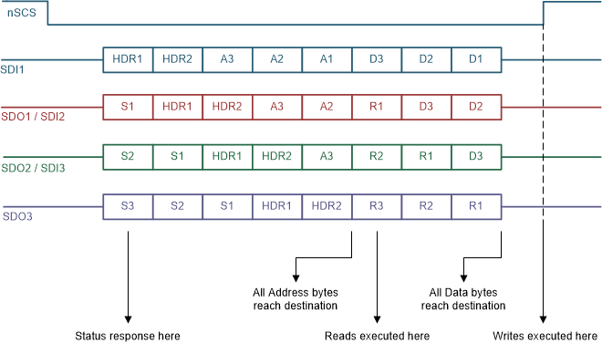
 Figure 7-50 SPI Frame With Three Devices
After the data has been transmitted through the chain, the MCU receives the data string in the format shown in Figure 7-51 for 3-device configuration: 3 bytes of status (Sx) followed by 2 bytes of header followed by 3 bytes of report (Rx).
 Figure 7-51 SPI Data Sequence for Three Devices
The header bytes contain information of the number of devices connected in the chain, and a global clear fault command that will clear the fault registers of all the devices on the rising edge of the chip select (nSCS) signal. Header values N5 through N0 are 6 bits dedicated to show the number of devices in the chain. Up to 63 devices can be connected in series for each daisy chain connection.
The 5 LSBs of the HDR2 register are don’t care bits that can be used by the MCU to determine integrity of the daisy chain connection. Header bytes must start with 1 and 0 for the two MSBs.
 Figure 7-52 Header Bytes
The status byte provides information about the fault status register for each device in the daisy chain so that the MCU does not have to initiate a read command to read the fault status from any particular device. This keeps additional read commands for the MCU and makes the system more efficient to determine fault conditions flagged in a device. Status bytes must start with 1 and 1 for the two MSBs.
 Figure 7-53 Contents of Header, Status, Address, and Data Bytes
When data passes through a device, it determines the position of itself in the chain by counting the number of status bytes it receives followed by the first header byte. For example, in this 3-device configuration, device 2 in the chain receives two status bytes before receiving the HDR1 byte which is then followed by the HDR2 byte.
From the two status bytes, the data can determine that its position is second in the chain. From the HDR2 byte, the data can determine how many devices are connected in the chain. In this way, the data only loads the relevant address and data byte in its buffer and bypasses the other bits. This protocol allows for faster communication without adding latency to the system for up to 63 devices in the chain.
The address and data bytes remain the same with respect to a 1-device connection. The report bytes (R1 through R3), as shown in Figure 7-51, are the content of the register being accessed.
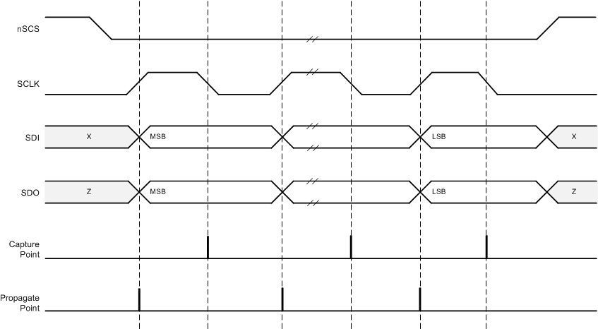
 Figure 7-54 SPI Transaction