SLOSE98A December 2022 – September 2023 DRV8461
PRODUCTION DATA
- 1
- 1 Features
- 2 Applications
- 3 Description
- 4 Revision History
- 5 Pin Configuration and Functions
- 6 Specifications
-
7 Detailed Description
- 7.1 Overview
- 7.2 Functional Block Diagram
- 7.3
Feature Description
- 7.3.1 Interface of Operation
- 7.3.2 Stepper Motor Driver Current Ratings
- 7.3.3 PWM Motor Drivers
- 7.3.4 Microstepping Indexer
- 7.3.5 Indexer Output
- 7.3.6 Automatic Microstepping Mode
- 7.3.7 Custom Microstepping Table
- 7.3.8 Current Regulation
- 7.3.9 Standstill Power Saving Mode
- 7.3.10 Current Regulation Decay Modes
- 7.3.11 Current Sensing with External Resistor
- 7.3.12 Silent step decay mode
- 7.3.13 Auto-torque Dynamic Current Adjustment
- 7.3.14 Charge Pump
- 7.3.15 Linear Voltage Regulator
- 7.3.16 VCC Voltage Supply
- 7.3.17 Logic Level, Tri-Level and Quad-Level Pin Diagrams
- 7.3.18 Spread Spectrum
- 7.3.19
Protection Circuits
- 7.3.19.1 VM Undervoltage Lockout
- 7.3.19.2 VCP Undervoltage Lockout (CPUV)
- 7.3.19.3 Logic Supply Power on Reset (POR)
- 7.3.19.4 Overcurrent Protection (OCP)
- 7.3.19.5 Stall Detection
- 7.3.19.6 Open-Load Detection (OL)
- 7.3.19.7 Overtemperature Warning (OTW)
- 7.3.19.8 Thermal Shutdown (OTSD)
- 7.3.19.9 Supply voltage sensing
- 7.3.19.10 nFAULT Output
- 7.3.19.11 Fault Condition Summary
- 7.3.20 Device Functional Modes
- 7.4 Programming
- 7.5
Register Maps
- 7.5.1 Status Registers
- 7.5.2
Control Registers
- 7.5.2.1 CTRL1 (address = 0x04) [Default = 0Fh]
- 7.5.2.2 CTRL2 (address = 0x05) [Default = 06h]
- 7.5.2.3 CTRL3 (address = 0x06) [Default = 38h]
- 7.5.2.4 CTRL4 (address = 0x07) [Default = 49h]
- 7.5.2.5 CTRL5 (address = 0x08) [Default = 03h]
- 7.5.2.6 CTRL6 (address = 0x09) [Default = 20h]
- 7.5.2.7 CTRL7 (address = 0x0A) [Default = FFh]
- 7.5.2.8 CTRL8 (address = 0x0B) [Default = 0Fh]
- 7.5.2.9 CTRL9 (address = 0x0C) [Default = 10h]
- 7.5.2.10 CTRL10 (address = 0x0D) [Default = 80h]
- 7.5.2.11 CTRL11 (address = 0x0E) [Default = FFh]
- 7.5.2.12 CTRL12 (address = 0x0F) [Default = 20h]
- 7.5.2.13 CTRL13 (address = 0x10) [Default = 10h]
- 7.5.2.14 CTRL14 (address = 0x3C) [Default = 58h]
- 7.5.3 Indexer Registers
- 7.5.4
Custom Microstepping Registers
- 7.5.4.1 CUSTOM_CTRL1 (address = 0x16) [Default = 00h]
- 7.5.4.2 CUSTOM_CTRL2 (address = 0x17) [Default = 00h]
- 7.5.4.3 CUSTOM_CTRL3 (address = 0x18) [Default = 00h]
- 7.5.4.4 CUSTOM_CTRL4 (address = 0x19) [Default = 00h]
- 7.5.4.5 CUSTOM_CTRL5 (address = 0x1A) [Default = 00h]
- 7.5.4.6 CUSTOM_CTRL6 (address = 0x1B) [Default = 00h]
- 7.5.4.7 CUSTOM_CTRL7 (address = 0x1C) [Default = 00h]
- 7.5.4.8 CUSTOM_CTRL8 (address = 0x1D) [Default = 00h]
- 7.5.4.9 CUSTOM_CTRL9 (address = 0x1E) [Default = 00h]
- 7.5.5
Auto torque Registers
- 7.5.5.1 ATQ_CTRL1 (address = 0x1F) [Default = 00h]
- 7.5.5.2 ATQ_CTRL2 (address = 0x20) [Default = 00h]
- 7.5.5.3 ATQ_CTRL3 (address = 0x21) [Default = 00h]
- 7.5.5.4 ATQ_CTRL4 (address = 0x22) [Default = 20h]
- 7.5.5.5 ATQ_CTRL5 (address = 0x23) [Default = 00h]
- 7.5.5.6 ATQ_CTRL6 (address = 0x24) [Default = 00h]
- 7.5.5.7 ATQ_CTRL7 (address = 0x25) [Default = 00h]
- 7.5.5.8 ATQ_CTRL8 (address = 0x26) [Default = 00h]
- 7.5.5.9 ATQ_CTRL9 (address = 0x27) [Default = 00h]
- 7.5.5.10 ATQ_CTRL10 (address = 0x28) [Default = 08h]
- 7.5.5.11 ATQ_CTRL11 (address = 0x29) [Default = 0Ah]
- 7.5.5.12 ATQ_CTRL12 (address = 0x2A) [Default = FFh]
- 7.5.5.13 ATQ_CTRL13 (address = 0x2B) [Default = 05h]
- 7.5.5.14 ATQ_CTRL14 (address = 0x2C) [Default = 0Fh]
- 7.5.5.15 ATQ_CTRL15 (address = 0x2D) [Default = 00h]
- 7.5.5.16 ATQ_CTRL16 (address = 0x2E) [Default = FFh]
- 7.5.5.17 ATQ_CTRL17 (address = 0x2F) [Default = 00h]
- 7.5.5.18 ATQ_CTRL18 (address = 0x30) [Default = 00h]
- 7.5.6 Silent Step Registers
- 8 Application and Implementation
- 9 Thermal Considerations
- 10Power Supply Recommendations
- 11Layout
- 12Device and Documentation Support
- 13Mechanical, Packaging, and Orderable Information
Package Options
Mechanical Data (Package|Pins)
Thermal pad, mechanical data (Package|Pins)
Orderable Information
8.2.2.1 Stepper Motor Speed
The first step in configuring the DRV8461 requires the desired motor speed and microstepping level. If the target application requires a constant speed, then a square wave with frequency ƒstep must be applied to the STEP pin. If the target motor speed is too high, the motor does not spin. Make sure that the motor can support the target speed. Use Equation 15 to calculate ƒstep for a desired motor speed (v), microstepping level (nm), and motor full step angle (θstep)
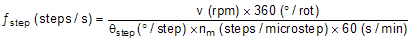
The value of θstep can be found in the stepper motor data sheet, or written on the motor. For example, the motor in this application is required to rotate at 1.8°/step for a target of 7.5 rpm at 1/16 microstep mode. Using Equation 15, ƒstep can be calculated as 400 Hz.
The microstepping level is set by the M0 and M1 pins or the MICROSTEP_MODE bits and can be any of the settings listed in Table 7-5. Higher microstepping results in a smoother motor motion and less audible noise, but requires a higher ƒstep to achieve the same motor speed.