SLOSE98A December 2022 – September 2023 DRV8461
PRODUCTION DATA
- 1
- 1 Features
- 2 Applications
- 3 Description
- 4 Revision History
- 5 Pin Configuration and Functions
- 6 Specifications
-
7 Detailed Description
- 7.1 Overview
- 7.2 Functional Block Diagram
- 7.3
Feature Description
- 7.3.1 Interface of Operation
- 7.3.2 Stepper Motor Driver Current Ratings
- 7.3.3 PWM Motor Drivers
- 7.3.4 Microstepping Indexer
- 7.3.5 Indexer Output
- 7.3.6 Automatic Microstepping Mode
- 7.3.7 Custom Microstepping Table
- 7.3.8 Current Regulation
- 7.3.9 Standstill Power Saving Mode
- 7.3.10 Current Regulation Decay Modes
- 7.3.11 Current Sensing with External Resistor
- 7.3.12 Silent step decay mode
- 7.3.13 Auto-torque Dynamic Current Adjustment
- 7.3.14 Charge Pump
- 7.3.15 Linear Voltage Regulator
- 7.3.16 VCC Voltage Supply
- 7.3.17 Logic Level, Tri-Level and Quad-Level Pin Diagrams
- 7.3.18 Spread Spectrum
- 7.3.19
Protection Circuits
- 7.3.19.1 VM Undervoltage Lockout
- 7.3.19.2 VCP Undervoltage Lockout (CPUV)
- 7.3.19.3 Logic Supply Power on Reset (POR)
- 7.3.19.4 Overcurrent Protection (OCP)
- 7.3.19.5 Stall Detection
- 7.3.19.6 Open-Load Detection (OL)
- 7.3.19.7 Overtemperature Warning (OTW)
- 7.3.19.8 Thermal Shutdown (OTSD)
- 7.3.19.9 Supply voltage sensing
- 7.3.19.10 nFAULT Output
- 7.3.19.11 Fault Condition Summary
- 7.3.20 Device Functional Modes
- 7.4 Programming
- 7.5
Register Maps
- 7.5.1 Status Registers
- 7.5.2
Control Registers
- 7.5.2.1 CTRL1 (address = 0x04) [Default = 0Fh]
- 7.5.2.2 CTRL2 (address = 0x05) [Default = 06h]
- 7.5.2.3 CTRL3 (address = 0x06) [Default = 38h]
- 7.5.2.4 CTRL4 (address = 0x07) [Default = 49h]
- 7.5.2.5 CTRL5 (address = 0x08) [Default = 03h]
- 7.5.2.6 CTRL6 (address = 0x09) [Default = 20h]
- 7.5.2.7 CTRL7 (address = 0x0A) [Default = FFh]
- 7.5.2.8 CTRL8 (address = 0x0B) [Default = 0Fh]
- 7.5.2.9 CTRL9 (address = 0x0C) [Default = 10h]
- 7.5.2.10 CTRL10 (address = 0x0D) [Default = 80h]
- 7.5.2.11 CTRL11 (address = 0x0E) [Default = FFh]
- 7.5.2.12 CTRL12 (address = 0x0F) [Default = 20h]
- 7.5.2.13 CTRL13 (address = 0x10) [Default = 10h]
- 7.5.2.14 CTRL14 (address = 0x3C) [Default = 58h]
- 7.5.3 Indexer Registers
- 7.5.4
Custom Microstepping Registers
- 7.5.4.1 CUSTOM_CTRL1 (address = 0x16) [Default = 00h]
- 7.5.4.2 CUSTOM_CTRL2 (address = 0x17) [Default = 00h]
- 7.5.4.3 CUSTOM_CTRL3 (address = 0x18) [Default = 00h]
- 7.5.4.4 CUSTOM_CTRL4 (address = 0x19) [Default = 00h]
- 7.5.4.5 CUSTOM_CTRL5 (address = 0x1A) [Default = 00h]
- 7.5.4.6 CUSTOM_CTRL6 (address = 0x1B) [Default = 00h]
- 7.5.4.7 CUSTOM_CTRL7 (address = 0x1C) [Default = 00h]
- 7.5.4.8 CUSTOM_CTRL8 (address = 0x1D) [Default = 00h]
- 7.5.4.9 CUSTOM_CTRL9 (address = 0x1E) [Default = 00h]
- 7.5.5
Auto torque Registers
- 7.5.5.1 ATQ_CTRL1 (address = 0x1F) [Default = 00h]
- 7.5.5.2 ATQ_CTRL2 (address = 0x20) [Default = 00h]
- 7.5.5.3 ATQ_CTRL3 (address = 0x21) [Default = 00h]
- 7.5.5.4 ATQ_CTRL4 (address = 0x22) [Default = 20h]
- 7.5.5.5 ATQ_CTRL5 (address = 0x23) [Default = 00h]
- 7.5.5.6 ATQ_CTRL6 (address = 0x24) [Default = 00h]
- 7.5.5.7 ATQ_CTRL7 (address = 0x25) [Default = 00h]
- 7.5.5.8 ATQ_CTRL8 (address = 0x26) [Default = 00h]
- 7.5.5.9 ATQ_CTRL9 (address = 0x27) [Default = 00h]
- 7.5.5.10 ATQ_CTRL10 (address = 0x28) [Default = 08h]
- 7.5.5.11 ATQ_CTRL11 (address = 0x29) [Default = 0Ah]
- 7.5.5.12 ATQ_CTRL12 (address = 0x2A) [Default = FFh]
- 7.5.5.13 ATQ_CTRL13 (address = 0x2B) [Default = 05h]
- 7.5.5.14 ATQ_CTRL14 (address = 0x2C) [Default = 0Fh]
- 7.5.5.15 ATQ_CTRL15 (address = 0x2D) [Default = 00h]
- 7.5.5.16 ATQ_CTRL16 (address = 0x2E) [Default = FFh]
- 7.5.5.17 ATQ_CTRL17 (address = 0x2F) [Default = 00h]
- 7.5.5.18 ATQ_CTRL18 (address = 0x30) [Default = 00h]
- 7.5.6 Silent Step Registers
- 8 Application and Implementation
- 9 Thermal Considerations
- 10Power Supply Recommendations
- 11Layout
- 12Device and Documentation Support
- 13Mechanical, Packaging, and Orderable Information
Package Options
Mechanical Data (Package|Pins)
Thermal pad, mechanical data (Package|Pins)
Orderable Information
7.3.19.6 Open-Load Detection (OL)
Open-load fault is detected -
When the motor is running -
If coil current drops below the open-load current threshold (IOL)
When the motor is in a holding condition -
If coil current drops below the ITRIP level set by the indexer
If either of the above conditions persists for more than the open-load detection time (tOL)
When the device is operating with SPI interface, the EN_OL bit must be 1b to enable open-load detection.
The open-load detection time (tOL) is set as shown in Table 7-27 -
Interface | OL_T | Maximum tOL (ms) |
|---|---|---|
H/W interface | NA | 60 |
SPI interface | 00b | 30 |
01b (default) | 60 | |
10b | 120 |
Once the open-load fault is detected -
nFAULT is pulled low.
If the device is operating with SPI interface -
OL and FAULT bits are latched 1b
If the OL_A bit is 1b, it indicates an open load fault in winding A, between AOUT1 and AOUT2.
An open load fault between BOUT1 and BOUT2 causes the OL_B bit to become 1b.
When the open-load condition is removed, the behavior depends on whether the device is configured with H/W interface or SPI interface.
When the device is configured with H/W interface and open-load condition is removed:
If the ENABLE pin is logic HIGH, nFAULT is released immediately.
If the ENABLE pin is Hi-Z, nFAULT is released after a nSLEEP reset pulse has been applied.
When the device is configured with SPI interface and open-load condition is removed:
If the OL_MODE bit is 1b, nFAULT is released immediately. OL bit in FAULT register and OL_X bits in DIAG2 register are cleared only after a clear faults command is issued either via the CLR_FLT bit or an nSLEEP reset pulse.
If the OL_MODE bit is 0b, nFAULT and the fault bits are released after a clear faults command is issued either via the CLR_FLT bit or an nSLEEP reset pulse.
The open-load fault also clears when the device is power cycled or comes out of sleep mode.
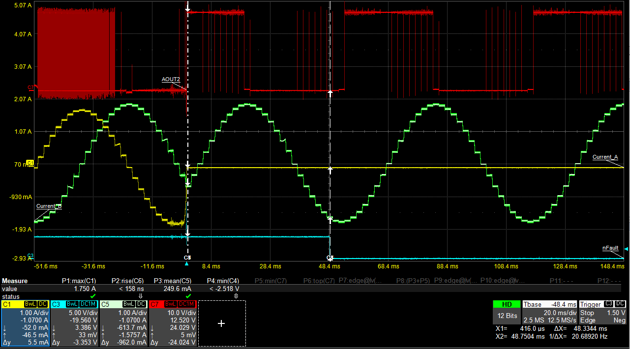
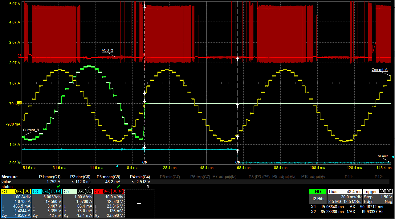
Figure 7-44 and Figure 7-45 show open-load detection in cases where coil A and coil B were opened respectively. The open load detection time was selected to be 60 ms maximum, and the OL_MODE bit was 0b.
 Figure 7-44 Coil A open-load detection. Traces from top to bottom: AOUT2, coil A current, coil B current, nFAULT
 Figure 7-45 Coil B open-load detection. Traces from top to bottom: AOUT2, coil A current, coil B current, nFAULT
In silent step decay mode, open-load fault detection works only if the motor is in motion. If the motor is in standstill, open-load detection is not supported.
When open-load fault is detected -
If ENABLE pin is changed from logic HIGH to Hi-Z on-the-fly, apply a nSLEEP reset pulse once the open-load condition is removed.
If OL_MODE is changed from 1b to 0b or EN_OL is changed from 1b to 0b, apply a clear faults command once the open-load condition is removed.
When the device is operating with auto-torque enabled, if open-load fault is detected, the coil current goes to a value corresponding to TRQ_DAC.