SLVSDR9E October 2016 – January 2021 DRV8702-Q1 , DRV8703-Q1
PRODUCTION DATA
- 1 Features
- 2 Applications
- 3 Description
- 4 Revision History
- 5 Pin Configuration and Functions
- 6 Specifications
-
7 Detailed Description
- 7.1 Overview
- 7.2 Functional Block Diagram
- 7.3
Feature Description
- 7.3.1 Bridge Control
- 7.3.2 MODE Pin
- 7.3.3 nFAULT Pin
- 7.3.4 Current Regulation
- 7.3.5 Amplifier Output (SO)
- 7.3.6 PWM Motor Gate Drivers
- 7.3.7 IDRIVE Pin (DRV8702-Q1 Only)
- 7.3.8 Dead Time
- 7.3.9 Propagation Delay
- 7.3.10 Overcurrent VDS Monitor
- 7.3.11 VDS Pin (DRV8702-Q1 Only)
- 7.3.12 Charge Pump
- 7.3.13 Gate Drive Clamp
- 7.3.14
Protection Circuits
- 7.3.14.1 VM Undervoltage Lockout (UVLO2)
- 7.3.14.2 Logic Undervoltage (UVLO1)
- 7.3.14.3 VCP Undervoltage Lockout (CPUV)
- 7.3.14.4 Overcurrent Protection (OCP)
- 7.3.14.5 Gate Driver Fault (GDF)
- 7.3.14.6 Thermal Shutdown (TSD)
- 7.3.14.7 Watchdog Fault (WDFLT, DRV8703-Q1 Only)
- 7.3.14.8 Reverse Supply Protection
- 7.3.15 Hardware Interface
- 7.4 Device Functional Modes
- 7.5 Programming
- 7.6 Register Maps
- 8 Application and Implementation
- 9 Power Supply Recommendations
- 10Layout
- 11Device and Documentation Support
- 12Mechanical, Packaging, and Orderable Information
Package Options
Refer to the PDF data sheet for device specific package drawings
Mechanical Data (Package|Pins)
- RHB|32
Thermal pad, mechanical data (Package|Pins)
Orderable Information
3 Description
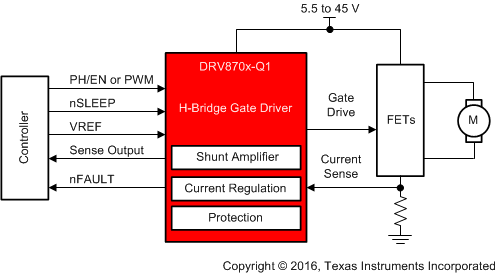
The DRV870x-Q1 devices are small single H-bridge gate drivers that use four external N-channel MOSFETs targeted to drive a bidirectional brushed-DC motor.
A PH/EN, independent H-Bridge, or PWM interface allows simple interfacing to controller circuits. An internal sense amplifier provides adjustable current control. Integrated Charge-Pump allows for 100% duty cycle support and can be used to drive external reverse battery switch.
Independent Half Bridge mode allows sharing of half bridges to control multiple DC motors sequentially in a cost-efficient way. The gate driver includes circuitry to regulate the winding current using fixed off-time PWM current chopping.
The DRV870x-Q1 devices include Smart Gate Drive technology to remove the need for any external gate components (resistors and Zener diodes) while protecting the external FETs. The Smart Gate Drive architecture optimizes dead time to avoid any shoot-through conditions, provides flexibility in reducing electromagnetic interference (EMI) with programmable slew-rate control and protects against any gate-short conditions. Additionally, active and passive pulldowns are included to prevent any dv/dt gate turn on.
| PART NUMBER | PACKAGE | BODY SIZE (NOM) |
|---|---|---|
| DRV8702-Q1 | VQFN (32) | 5.00 mm × 5.00 mm |
| DRV8703-Q1 |
 Simplified Schematic