SLVSAW5D July   2011  – December 2024 DRV8803

PRODUCTION DATA  

  1.   1
  2. Features
  3. Applications
  4. Description
  5. Device Comparison
  6. Pin Configuration and Functions
    1.     Pin Functions
  7. Specification
    1. 6.1 Absolute Maximum Ratings
    2. 6.2 ESD Ratings
    3. 6.3 Recommended Operating Conditions
    4. 6.4 Thermal Information
    5. 6.5 Electrical Characteristics
    6. 6.6 Timing Requirements
    7. 6.7 Typical Characteristics
  8. Detailed Description
    1. 7.1 Overview
    2. 7.2 Functional Block Diagram
    3. 7.3 Feature Description
      1. 7.3.1 Output Drivers
      2. 7.3.2 Protection Circuits
        1. 7.3.2.1 Overcurrent Protection (OCP)
        2. 7.3.2.2 Thermal Shutdown (TSD)
        3. 7.3.2.3 Undervoltage Lockout (UVLO)
    4. 7.4 Device Functional Modes
      1. 7.4.1 Parallel Interface Operation
      2. 7.4.2 nENBL and RESET Operation
  9. Application and Implementation
    1. 8.1 Application Information
      1. 8.1.1 Application as Load driver
        1. 8.1.1.1 Design Requirements
        2. 8.1.1.2 Detailed Design Procedure
          1. 8.1.1.2.1 Supply Voltage
          2. 8.1.1.2.2 Load Current
            1. 8.1.1.2.2.1 Peak Current
            2. 8.1.1.2.2.2 Hold Current
            3. 8.1.1.2.2.3 Frequency
        3. 8.1.1.3 Application Curves
      2. 8.1.2 Application as Unipolar Stepper Driver
        1. 8.1.2.1 Design Requirements
        2. 8.1.2.2 Detailed Design Procedure
          1. 8.1.2.2.1 Motor Voltage
          2. 8.1.2.2.2 Drive Current
        3. 8.1.2.3 Application Curves
    2.     Power Supply Recommendations
      1. 8.2.1 Bulk Capacitance
    3. 8.2 Layout
      1. 8.2.1 Layout Guidelines
      2. 8.2.2 Layout Example
      3. 8.2.3 Thermal Consideration
        1. 8.2.3.1 Thermal Protection
        2. 8.2.3.2 Power Dissipation
        3. 8.2.3.3 Heatsinking
  10. Device and Documentation Support
    1. 9.1 Documentation Support
      1. 9.1.1 Related Documentation
    2. 9.2 Community Resources
    3. 9.3 Trademarks
  11. 10Revision History
  12. 11Mechanical, Packaging, and Orderable Information

Package Options

Mechanical Data (Package|Pins)
Thermal pad, mechanical data (Package|Pins)
Orderable Information

Application Curves

DRV8803 Current Ramp With a 16Ω, 1mH RL Load and VM = 8.2VFigure 8-4 Current Ramp With a 16Ω, 1mH RL Load and VM = 8.2V
DRV8803 OCP With VM = 8.2V and OUT1 Shorted to VMFigure 8-6 OCP With VM = 8.2V and OUT1 Shorted to VM
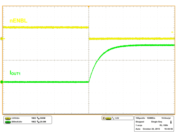
DRV8803 Current Ramp With a 16Ω, 1mH RL Load and VM = 30VFigure 8-5 Current Ramp With a 16Ω, 1mH RL Load and VM = 30V
DRV8803 OCP Separated by tRETRY With VM = 8.2V and OUT1 Shorted to VMFigure 8-7 OCP Separated by tRETRY With VM = 8.2V and OUT1 Shorted to VM